Atomic Force Microscopy in Cleaning Validation: A High-Resolution Approach for Optical Components and Biomedical Applications
This article explores the critical application of Atomic Force Microscopy (AFM) for the cleaning validation of optical components and laboratory equipment, a vital process in pharmaceutical manufacturing and biomedical research.
Atomic Force Microscopy in Cleaning Validation: A High-Resolution Approach for Optical Components and Biomedical Applications
Abstract
This article explores the critical application of Atomic Force Microscopy (AFM) for the cleaning validation of optical components and laboratory equipment, a vital process in pharmaceutical manufacturing and biomedical research. It establishes the foundational role of AFM in directly characterizing nanoscale surface contamination and cleaning efficacy, moving beyond indirect measurements. A detailed methodological framework for using AFM in cleaning validation protocols is provided, including practical procedures for sample preparation, imaging, and data analysis. The content addresses common troubleshooting challenges and optimization strategies to ensure reliable AFM data. Finally, it validates AFM's superiority by comparing its capabilities with other analytical techniques and demonstrating its synergy with methods like Total Organic Carbon (TOC) analysis and LC-MS/MS, offering a comprehensive lifecycle approach to contamination control.
The Foundational Role of AFM in Nanoscale Surface Characterization
Defining Cleaning Validation and Its Critical Importance in Pharmaceutical and Optical Industries
Cleaning validation is a critical quality assurance process that provides documented evidence that a cleaning procedure consistently and effectively removes product residues, contaminants, and cleaning agents from equipment surfaces to prevent cross-contamination [1] [2]. In both pharmaceutical and optical industries, this process ensures that equipment is properly cleaned prior to use, thereby safeguarding product safety, efficacy, and quality [3] [4]. The fundamental objective of any validation process is to demonstrate through scientific data that the system consistently performs as expected and meets predetermined specifications [3].
The consequences of inadequate cleaning procedures can be severe. Historically, the U.S. Food and Drug Administration (FDA) has documented numerous contamination incidents, including a significant 1988 recall of a finished drug product, Cholestyramine Resin USP, where the bulk pharmaceutical chemical became contaminated with intermediates and degradants from agricultural pesticide production due to inadequate solvent control and cleaning procedures [3]. Similarly, in optical manufacturing, improper cleaning can cause scattering effects, damage to optical coatings, and compromised performance of sensitive components [4].
Cleaning Validation in the Pharmaceutical Industry
Regulatory Framework and Requirements
The pharmaceutical industry operates under stringent regulatory requirements for cleaning validation. The FDA's 1978 CGMP regulations explicitly addressed equipment cleaning in Section 211.67, establishing clear expectations for pharmaceutical manufacturers [3]. While the FDA does not set specific acceptance specifications or methods due to the wide variation in equipment and products, it provides a framework of expectations that manufacturers must meet [3].
Regulatory agencies generally expect pharmaceutical manufacturers to have:
- Written procedures (SOPs) detailing cleaning processes for various equipment [3]
- General validation procedures specifying responsibility, acceptance criteria, and revalidation requirements [3]
- Specific validation protocols for each manufacturing system or piece of equipment [3]
- Documented validation studies conducted in accordance with established protocols [3]
- Final validation reports approved by management [3]
Acceptance Criteria and Limits
Establishing scientifically justifiable acceptance criteria is fundamental to cleaning validation. The pharmaceutical industry typically employs multiple parameters to evaluate cleaning effectiveness:
Table 1: Pharmaceutical Cleaning Validation Acceptance Criteria
| Criterion Type | Specific Limits | Application Context |
|---|---|---|
| Chemical | ≤ 10 ppm of a product in another product [1] | General cross-contamination limit |
| Biological Activity | ≤ 0.1% of normal therapeutic dose [3] [1] | Based on product potency |
| Microbial | ≤ 20 CFU for bacterial counts [1] | Bioburden control |
| Physical | No visible residues [3] | Basic requirement for all equipment |
The Maximum Allowable Carryover (MACO) is typically calculated using the formula: MACO = (NOEL × MBS) / (SF × TDD), where NOEL is the No Observed Effect Level, MBS is the Maximum Batch Size, SF is a Safety Factor (typically 1000 for oral drugs), and TDD is the Total Daily Dose of the next product [2].
Sampling and Analytical Methods
Pharmaceutical cleaning validation employs two primary sampling approaches:
Direct Sampling (Swab Method): A sterile material is systematically rubbed across a surface to be analyzed for residue presence [1]. This method is particularly useful for hard-to-clean areas and provides direct measurement of residual contamination on specific equipment surfaces [2].
Indirect Sampling (Rinse Sampling): A solvent is rinsed across clean equipment surfaces and tested for contaminant traces [1]. This approach is valuable for inaccessible areas or large surface areas [2].
Analytical methods commonly used include High-Performance Liquid Chromatography (HPLC), Total Organic Carbon (TOC) analysis, UV-Vis spectroscopy, and microbiological testing [2]. These methods must be validated for specificity, sensitivity, and accuracy to ensure reliable results [2].
Cleaning Validation in the Optical Industry
Unique Requirements for Optical Components
Optical components present distinct cleaning challenges compared to pharmaceutical equipment. Dust, stains, and impurities on optical surfaces can cause light scattering, while contaminants can react with incident laser light to damage sensitive optical coatings [4]. The precision required for optical surfaces often exceeds general industrial cleaning standards, with even microscopic residues potentially compromising performance.
Optical cleaning validation must account for the extreme sensitivity of certain optical surfaces, including holographic and ruled gratings, first-surface unprotected metallic mirrors, and pellicle beamsplitters, which can be damaged by any physical contact from hands or optical handling instruments [4]. The validation approach must therefore balance cleaning effectiveness with the potential for damaging delicate surfaces during the cleaning process.
Optical Cleaning Techniques and Validation
The optical industry employs specialized cleaning techniques tailored to different component types and contamination levels:
Table 2: Optical Cleaning Techniques and Applications
| Technique | Procedure | Suitable For | Precautions |
|---|---|---|---|
| Drop and Drag [4] | Place unfolded lens tissue over optic, add solvent, slowly drag tissue across surface | Unmounted optics, mirrors, beam pick-offs | Avoid abrasive surfaces |
| Brush Technique [4] | Create lens-tissue brush, wet with solvent, wipe slowly across optic surface | Small optics, beamsplitter cubes, mounted components | Avoid getting solvent into prism gaps |
| Immersion Technique [4] | Immerse optic in solvent, potentially with ultrasonic agitation | Softer coatings, Nanotexture windows and lenses | Never use for cemented optics |
| Polymer Film [4] | Apply designer polymer that dries to a film, then peel off | Rough surfaces, gratings, atomic-level cleaning | Not for Nanotexture surfaces |
| Vapor Degreasing [5] | Use specialized solvents in controlled vapor degreasing equipment | Complex optical parts with waxes, oils, greases | Requires specialized equipment |
Validation of optical cleaning typically involves both visual inspection under bright lighting to detect scattering from dust and stains [4], and for precision applications, potentially advanced techniques such as atomic-level analysis to verify surface integrity.
Comparative Analysis: Pharmaceutical vs. Optical Cleaning Validation
Methodology Comparison
While both industries share the fundamental goal of preventing contamination, their approaches to cleaning validation differ significantly based on their unique requirements and risks.
Table 3: Pharmaceutical vs. Optical Cleaning Validation
| Parameter | Pharmaceutical Industry | Optical Industry |
|---|---|---|
| Primary Concern | Chemical and microbial contamination affecting patient safety [3] [1] | Surface residues affecting optical performance and coating integrity [4] |
| Validation Focus | Chemical residues, cleaning agents, microorganisms [2] | Particulates, films, hydrocarbons, surface integrity [4] [5] |
| Sampling Methods | Swab and rinse sampling with laboratory analysis [1] | Visual inspection, optical performance testing, advanced surface analysis [4] |
| Analytical Techniques | HPLC, TOC, UV-Vis, microbial tests [2] | Visual inspection, scattering analysis, polymer film residue detection [4] |
| Acceptance Criteria | Quantitative limits (ppm, microbial counts) [1] | Visual cleanliness, performance metrics, surface integrity [4] |
| Regulatory Framework | FDA CGMP, detailed documentation requirements [3] | Industry standards, manufacturer specifications [4] |
Emerging Technologies and Advanced Methodologies
Both industries are adopting advanced technologies to improve cleaning validation:
Process Analytical Technology (PAT) in pharmaceuticals enables real-time monitoring of cleaning processes through techniques like Raman spectroscopy and optical imaging, significantly reducing solvent usage and improving efficiency [6]. Near Infra-Red Chemical Imaging (NIR-CI) shows promise for detecting API and detergent residues on equipment surfaces in real-time, potentially revolutionizing cleaning verification by providing both spectral and spatial information simultaneously [7].
For optical applications, UV/ozone cleaning offers a method for removing microscopic contaminants and organic layers from sensitive surfaces without physical contact, making it particularly valuable for AFM reference and calibration samples [8]. This technique uses short-wavelength UV light to produce ozone, which acts as a strong oxidizing agent to decompose organic contaminants [8].
Advanced Applications: Atomic Force Microscopy in Cleaning Validation
AFM for Cleaning Validation Research
Atomic force microscopy (AFM) represents a powerful tool for cleaning validation research in both pharmaceutical and optical contexts. AFM enables nanoscale characterization of surface cleanliness, providing insights beyond conventional validation methods. For pharmaceutical applications, AFM can detect and quantify residual films and particulate contamination on equipment surfaces that might harbor microorganisms or chemical residues [8].
In optical cleaning validation, AFM can directly image and measure surface contaminants that affect optical performance, providing quantitative data on surface roughness, particulate distribution, and coating integrity before and after cleaning procedures. This capability is particularly valuable for validating cleaning methods for sensitive optical components where conventional sampling methods might damage surfaces.
Specialized Cleaning Methods for AFM Components
Cleaning AFM components themselves requires specialized approaches. Standard cleaning methods involving swabbing or wiping can irreparably damage sensitive AFM calibration specimens [8]. The "New Skin" technique provides an alternative for removing large contaminants without mechanical damage to these sensitive surfaces [8]. This method can be combined with UV/ozone cleaning to achieve near-perfect cleaning for AFM reference artifacts [8].
The workflow for AFM-related cleaning validation can be visualized as follows:
Research Reagent Solutions for AFM Cleaning Studies
The following reagents and materials are essential for conducting AFM-related cleaning validation research:
Table 4: Research Reagent Solutions for AFM Cleaning Validation
| Reagent/Material | Function | Application Context |
|---|---|---|
| New Skin polymer [8] | Removes macroscopic contamination without mechanical damage | AFM calibration specimens, sensitive surfaces |
| UV/Ozone system [8] | Removes microscopic organic contaminants through oxidation | Organic layer removal, hydrocarbon contamination |
| Spectrophotometric-grade solvents [4] | High-purity cleaning without residual impurities | Precision optical components, analytical surfaces |
| Low-lint lens tissue [4] | Gentle wiping without scratching or leaving residues | Delicate optical surfaces, mirrored coatings |
| Polymer film cleaners [4] | Atomic-level cleaning through encapsulation | Ultimate surface cleanliness, rough textures |
| AeroTron-AV solvent [5] | Vapor degreasing for production contaminants | Complex optical parts, wax and grease removal |
Cleaning validation serves as a critical quality assurance process in both pharmaceutical and optical industries, though with different applications, methodologies, and acceptance criteria. The pharmaceutical industry emphasizes regulatory compliance, chemical residue limits, and documentation rigor to ensure patient safety [3] [1] [2], while the optical industry focuses on surface integrity, particulate removal, and optical performance preservation [4] [9].
Advanced techniques including Process Analytical Technology, Near Infra-Red Chemical Imaging, and atomic force microscopy are transforming cleaning validation practices in both fields [7] [6]. These technologies enable more precise, real-time monitoring of cleaning effectiveness and provide deeper understanding of cleaning mechanisms. For researchers working at the intersection of AFM and cleaning validation, specialized methodologies that avoid surface damage while achieving requisite cleanliness levels are essential for accurate results and equipment preservation [8].
As both industries continue to evolve, the convergence of validation approaches through technological advancement may lead to more robust, efficient, and scientifically grounded cleaning validation protocols that further enhance product quality and performance across multiple sectors.
In both pharmaceutical development and optical component manufacturing, surface properties dictate product performance, stability, and safety. Traditional quality control often relies on visual inspection or conventional analytical techniques that provide only bulk composition data, failing to detect critical nanoscale variations. These methods cannot characterize the three-dimensional topography, mechanical properties, or chemical distribution at the nanometer scale, where many performance-critical phenomena occur [10] [11].
Atomic force microscopy (AFM) has emerged as a powerful solution that transcends these limitations by providing direct, quantitative surface analysis under ambient or physiological conditions. Unlike electron microscopy techniques that require vacuum environments and extensive sample preparation, AFM generates three-dimensional topography maps with nanoscale resolution while simultaneously quantifying mechanical, chemical, and functional properties [10] [12]. This capability makes AFM indispensable for validating cleaning processes for optical components and optimizing drug formulations where surface characteristics directly correlate with performance.
Comparative Analysis of Surface Analysis Techniques
Technical Capabilities Comparison
The table below compares the key characteristics of AFM against other surface analysis techniques:
Table 1: Comparison of Surface Analysis Techniques for Pharmaceutical and Optical Applications
| Technique | Resolution | Sample Environment | Quantitative Data | Sample Preparation | Key Limitations |
|---|---|---|---|---|---|
| Atomic Force Microscopy (AFM) | ~5 nm topographic [13] | Ambient, liquid, or controlled conditions [10] | 3D topography, mechanical properties, adhesion forces [10] [12] | Minimal [10] | Limited scan area, tip wear potential |
| Scanning Electron Microscopy (SEM) | ~1 nm | High vacuum required | 2D images, elemental composition (with EDS) | Extensive (conductive coating often needed) | No direct 3D data, no mechanical properties [10] |
| Time-of-Flight SIMS (ToF-SIMS) | ~100 nm chemical [11] | High vacuum | Chemical composition, molecular distribution | Minimal for surface analysis | Limited topographic information, semi-quantitative |
| X-ray Photoelectron Spectroscopy (XPS) | ~10 μm [11] | Ultra-high vacuum | Elemental composition, chemical states | Minimal for surface analysis | Very limited topographic information |
| Optical Profilometry | ~200 nm vertical | Ambient | 3D topography, roughness parameters | Minimal | Limited lateral resolution, no mechanical properties |
Quantitative Performance Data
Recent studies demonstrate AFM's capabilities in providing quantitative data essential for research and development:
Table 2: Quantitative AFM Performance in Applied Research Settings
| Application Area | Measured Parameters | Results | Significance |
|---|---|---|---|
| Optical Component Cleaning Validation | Surface roughness, organic contaminant removal | Complete performance restoration after low-pressure plasma cleaning [14] | Direct correlation between cleaning efficacy and laser-induced damage threshold |
| Pharmaceutical Tablet Analysis | Surface roughness, domain distribution, mechanical properties | Distinct drug distribution patterns in 4 mg vs. 0.5 mg dexamethasone tablets [11] | Revealed formulation heterogeneity affecting drug release kinetics |
| Nanoparticle Drug Loading | Drug distribution mapping, individual NP quantification | Drug loading varied from 0-21 wt% between individual nanoparticles [15] | Unprecedented quantification of formulation heterogeneity at single-particle level |
| Crystal Growth Monitoring | Real-time crystal growth kinetics, defect formation | Observed significant crystal growth on amorphous nifedipine surfaces under ambient conditions [10] | Critical for predicting drug stability and shelf life |
Experimental Protocols for AFM Analysis
Nanomechanical Characterization of Soft Materials
For reliable nanomechanical characterization of soft materials including pharmaceutical components and optical coatings, the following protocol provides a framework for reproducible measurements [12]:
AFM Mode Selection: Choose appropriate operation mode based on sample properties:
- Intermittent Contact Mode: Ideal for topographical imaging of soft, adhesive, or loosely-bound samples
- Nanomechanical Imaging: Provides simultaneous topography and property mapping
- Force Modulation: Characterizes viscoelastic properties through controlled tip-sample interactions
- Force Spectroscopy: Quantifies adhesion forces, mechanical properties at specific locations
Cantilever Selection and Calibration:
- Select cantilevers with spring constants appropriate for sample stiffness (typically 0.1-5 N/m for soft materials)
- Use thermal tuning method to determine precise spring constant and sensitivity
- Choose tips with appropriate geometry (sharp tips for high resolution, colloidal probes for mechanical tests)
Sample Preparation:
- For tablet surface analysis, analyze intact tablets without cutting to preserve native surface structure [11]
- For nanoparticle characterization, deposit dilute suspensions on freshly cleaved mica or silicon substrates
- Ensure secure mounting to minimize acoustic and vibrational noise
Measurement Optimization:
- Set appropriate scan rates (typically 0.5-1.5 Hz) to balance resolution and fidelity
- Optimize feedback parameters to maintain consistent tip-sample interaction
- Perform measurements in controlled environments (temperature, humidity) when comparing samples
Data Analysis and Reporting:
- Apply appropriate flattening algorithms to remove sample tilt and bow
- Use consistent thresholding for particle analysis and roughness calculations
- Report key parameters including resolution, scan rate, cantilever properties, and processing methods
AFM-IR for Drug Distribution Quantification
The AFM-IR technique combines AFM's spatial resolution with infrared spectroscopy's chemical specificity, enabling drug quantification in individual nanoparticles [15]:
Calibration Curve Establishment:
- Prepare homogeneous thin films of polymer and drug with known compositions
- Acquire IR spectra using conventional microspectroscopy for reference
- Establish correlation between IR absorption intensity and drug concentration
Sample Preparation for AFM-IR:
- Deposit nanoparticle suspension on gold-coated substrates or IR-transparent prisms
- Ensure isolated, well-distributed nanoparticles for single-particle analysis
- Use tapping mode to prevent sample displacement during measurement
Spectral Acquisition and Mapping:
- Operate AFM-IR in top-down illumination configuration with tapping mode
- Tune IR laser to specific absorption bands of drug and polymer matrix
- Acquire local IR spectra at multiple points within individual nanoparticles
- Generate chemical maps based on specific absorption intensities
Drug Loading Quantification:
- Apply calibration curve to convert AFM-IR signal intensities to drug concentrations
- Calculate drug loading for individual nanoparticles
- Perform statistical analysis across multiple nanoparticles to assess batch heterogeneity
AFM in Optical Component Cleaning Validation
Protocol for Cleaning Efficacy Assessment
The validation of cleaning processes for optical components requires direct assessment of surface topography and contamination removal:
Pre-Cleaning Characterization:
- Acquire AFM topography images of multiple representative areas (typically 5×5 μm to 20×20 μm)
- Measure root mean square (RMS) roughness and surface skewness
- Perform phase imaging to identify organic contaminant regions
Cleaning Process Application:
- Apply low-pressure plasma cleaning or other cleaning methodologies
- Vary cleaning parameters (time, power, gas composition) for optimization
Post-Cleaning Analysis:
- Re-measure identical surface locations when possible
- Quantify reduction in surface roughness and removal of particulate contaminants
- Assess changes in adhesion forces using force spectroscopy
Correlation with Functional Performance:
- Correlate AFM measurements with laser-induced damage threshold testing
- Relate surface topography changes to optical transmittance measurements [14]
The Scientist's Toolkit: Essential Research Reagents and Materials
Table 3: Essential Research Materials for AFM Surface Analysis
| Material/Component | Function/Application | Key Specifications | Considerations |
|---|---|---|---|
| Silicon AFM Probes | Topographical imaging in tapping mode | Tip radius: ~5 nm, Resonance frequency: ~70 kHz, Spring constant: 1.7 N/m [11] | Match spring constant to sample stiffness; sharper tips for higher resolution |
| Silicon Cantilevers for AFM-IR | Chemical mapping via photothermal expansion | Rectangular cantilevers, Specific dimensions for IR laser detection [15] | Ensure compatibility with AFM-IR instrumentation |
| Poly(lactic acid) Nanoparticles | Drug delivery system model | Size: 200-300 nm, Biocompatible, biodegradable [15] | Standard model for method development and validation |
| Reference Standards | Calibration and quantification | Well-characterized composition (e.g., dexamethasone USP standard) [11] | Essential for quantitative analysis and method validation |
| Specialized Substrates | Sample support for AFM measurement | Mica, silicon wafers, gold-coated slides [15] | Atomically flat surfaces for high-resolution imaging |
| Gas Cluster Ion Beam Source | Depth profiling for ToF-SIMS | Ar1000+ clusters, 10 keV energy [11] | Enables non-destructive 3D chemical analysis combined with AFM |
Atomic force microscopy represents a paradigm shift in surface characterization, moving beyond qualitative visual assessment to direct, quantitative analysis with nanoscale resolution. The experimental protocols and comparative data presented demonstrate AFM's unique capability to correlate surface properties with functional performance in both pharmaceutical development and optical component manufacturing.
The integration of AFM with complementary techniques such as AFM-IR and ToF-SIMS creates a powerful analytical framework for understanding complex surface phenomena. As fabrication technologies advance, producing ultra-sharp probes with precisely controlled geometries [13], AFM's applications continue to expand, enabling researchers to solve increasingly challenging problems in surface science and engineering.
For researchers and product developers, adopting these direct quantitative analysis methods provides critical insights that drive innovation, enhance product quality, and accelerate development timelines across multiple industries dependent on precise surface engineering.
Atomic Force Microscopy (AFM) stands as a cornerstone technique in nanoscale surface metrology, providing unparalleled three-dimensional topographic data. Its unique capability to quantitatively measure surface features with sub-nanometer resolution makes it indispensable for advanced materials characterization, particularly in precision-sensitive fields such as optical component manufacturing and cleaning validation research. Unlike optical microscopes, which are limited by the diffraction of light to approximately 0.2 micrometers, AFM achieves atomic-level resolution by employing a physical probe that raster-scans the sample surface [16] [17]. This mechanical probing overcomes the limitations of optical diffraction and electron microscopy's two-dimensional imaging, enabling true topographic mapping essential for validating surface treatments and cleaning processes on optical components [18] [14]. For researchers focused on optical component cleaning, AFM provides the critical capability to directly assess nanoscale contamination status and cleaning effectiveness, offering quantitative data on surface roughness and topography that correlates with optical performance metrics such as transmittance and laser-induced damage threshold [14].
Fundamental Principles of AFM Operation
Core Components and Their Functions
The atomic force microscope operates through an integrated system of key components that work in concert to probe surface topography:
Scanning System: Typically employing piezoelectric tubes or electromagnetic actuators, this system provides precise nanoscale motion in X, Y, and Z directions, enabling raster scanning of the probe across the sample surface with sub-Ångstrom precision [17] [19].
Probe Assembly: Consisting of a sharp tip (with typical radius of curvature of 5-10 nm) mounted on a flexible cantilever, this assembly physically interacts with the sample surface. Cantilevers are typically fabricated from silicon or silicon nitride, with dimensions carefully engineered to achieve specific spring constants according to the formula: k = Ewt³/4L³, where w is width, t is thickness, L is length, and E is Young's modulus [19].
Detection System: Employs an optical beam deflection method where a laser beam reflects off the cantilever onto a position-sensitive photodetector (PSPD). Nanoscale deflections of the cantilever alter the laser's path, allowing the PSPD to track both vertical and lateral motions with <0.01 nm accuracy [19] [20].
Feedback Control: Continuously monitors tip-sample interaction forces and adjusts the Z-position to maintain a constant setpoint value (either deflection or oscillation amplitude). This closed-loop system, typically implemented through proportional-integral-derivative (PID) control, ensures consistent tracking of surface topography despite variations in sample height [16] [19].
Controller Electronics and Computer: Interface between the hardware components and provide real-time data acquisition, processing, and image display capabilities [17].
Primary Operational Modes
AFM operates in several distinct modes, each optimized for specific sample types and measurement requirements:
Contact Mode: The most fundamental AFM mode where the tip maintains perpetual contact with the sample surface. The feedback loop maintains constant cantilever deflection during scanning, corresponding to a constant force applied to the sample. While providing high resolution, this mode can exert significant shear forces that may damage soft samples [21] [17].
Tapping Mode (also called Dynamic or Intermittent Contact Mode): The cantilever is oscillated at or near its resonance frequency, causing the tip to intermittently contact the surface. The feedback system maintains constant oscillation amplitude during scanning. This mode significantly reduces lateral forces and sample damage, making it suitable for soft materials including polymers, biological samples, and delicate optical coatings [16] [18].
Non-Contact Mode: The cantilever oscillates just above the sample surface without making physical contact, sensing only attractive van der Waals forces. While minimizing tip and sample wear, this mode offers lower resolution and can be less stable than other modes [21] [17].
Table 1: Comparison of Primary AFM Operational Modes
| Operating Mode | Tip-Sample Interaction | Best For | Limitations |
|---|---|---|---|
| Contact Mode | Perpetual physical contact | Hard, robust samples (semiconductors, ceramics) | High shear forces may damage soft samples |
| Tapping Mode | Intermittent contact | Soft, delicate, or adhesive samples (polymers, biological cells) | Slower scan speeds; potential for tip wear |
| Non-Contact Mode | Attractive forces only | Mapping long-range forces (electrical, magnetic) | Lower resolution; less stable operation |
Advanced AFM Techniques for Comprehensive Surface Characterization
Beyond basic topography imaging, AFM offers specialized modes that extract additional surface properties valuable for optical component research:
Phase Imaging: Maps variations in surface composition, adhesion, and viscoelastic properties by monitoring the phase lag between the driving oscillation and cantilever response in tapping mode [17].
Force Modulation Microscopy (FMM): Assesses local stiffness and elasticity by applying high-frequency oscillations to the cantilever while scanning and monitoring amplitude changes indicative of surface hardness [21].
Lateral Force Microscopy (LFM): Measures frictional forces between tip and sample by monitoring torsional deflections of the cantilever as it scans across the surface [21].
Scanning Thermal Microscopy (SThM): Maps thermal properties and temperature distribution across a surface using a thermally-sensitive probe [21] [17].
Electric Force Microscopy (EFM) and Magnetic Force Microscopy (MFM): Use a two-pass "LiftMode" technique to separately map topographic features and long-range electrical or magnetic forces [21] [17].
These advanced techniques enable researchers to correlate surface topography with material properties, providing comprehensive characterization of optical components before and after cleaning processes.
Key Metrics for Surface Topography Analysis
AFM provides quantitative, three-dimensional data enabling precise calculation of surface roughness parameters essential for optical component validation. Unlike qualitative methods, AFM measures X, Y, and Z dimensions with resolutions of 2-10 nm laterally and sub-nanometer vertically [22] [17]. The most common roughness parameters are derived from statistical analysis of height deviations from a mean plane:
Arithmetical Mean Height (Sa): The average absolute deviation of surface heights from the mean plane, calculated as Sa = (1/A)∬|Z(x,y)|dxdy, where A is the defined area [22].
Root Mean Square Height (Sq): The standard deviation of height distribution, calculated as Sq = √[(1/A)∬Z²(x,y)dxdy]. This parameter gives higher weight to extreme values [22].
Skewness (Ssk): Measures asymmetry of the height distribution histogram, calculated as Ssk = (1/Sq³)[(1/A)∬Z³(x,y)dxdy]. Positive values indicate predominance of peaks, while negative values suggest predominance of valleys [22].
Kurtosis (Sku): Quantifies the "peakedness" or sharpness of the height distribution, calculated as Sku = (1/Sq⁴)[(1/A)∬Z⁴(x,y)dxdy]. A Gaussian surface has Sku = 3, while higher values indicate more extreme height variations [22].
For optical applications, these parameters directly influence performance characteristics. For instance, sapphire or glass surfaces polished to sub-nanometer roughness (Sa = 0.12 nm) minimize light scattering, while increased skewness and kurtosis values indicate contamination particles that can compromise optical performance [22].
Table 2: Key Surface Roughness Parameters and Their Significance for Optical Components
| Parameter | Definition | Optical Performance Significance |
|---|---|---|
| Sa | Arithmetical mean height deviation | Low values minimize diffuse scattering; high values increase light loss |
| Sq | Root mean square roughness | More sensitive to outlier peaks/valleys that cause localized scattering |
| Ssk | Skewness (asymmetry of height distribution) | Positive values (peak-dominated) increase forward scattering; negative values (valley-dominated) may trap contaminants |
| Sku | Kurtosis (sharpness of height distribution) | High values indicate extreme peaks/valleys that create localized electric field enhancements |
Experimental Protocols for Optical Component Cleaning Validation
Sample Preparation and Mounting
Proper sample preparation is critical for reliable AFM analysis of optical components:
Cleaning Protocol: Prior to initial measurement, clean optical components using appropriate methods (e.g., low-pressure plasma cleaning for organic contaminant removal) [14].
Mounting Procedure: Securely mount samples to the AFM stage using compatible adhesives or holders to minimize vibration during scanning. Ensure the surface is approximately perpendicular to the probe approach axis.
Reference Samples: Include standardized roughness samples for periodic verification of instrument calibration and measurement consistency.
AFM Imaging Parameters
Optimal parameter selection ensures accurate topography representation:
Scan Size and Resolution: Typical scan sizes range from 1×1 μm to 100×100 μm, with pixel resolution of 256×256 to 1024×1024, balancing field of view with detail.
Scan Rate: Adjust between 0.5-2 Hz to optimize tracking while minimizing thermal drift and acquisition time [19].
Setpoint and Gains: For tapping mode, set amplitude setpoint to 80-90% of free oscillation amplitude. Carefully adjust PID gains to minimize noise while maintaining adequate surface tracking [19].
Tip Selection: Choose tips with appropriate radius, aspect ratio, and spring constant based on surface features. Sharp tips (5-10 nm radius) are essential for high-resolution imaging of nanoscale contaminants [19].
Data Acquisition and Processing
Standardized processing ensures comparable results across measurements:
Image Leveling: Apply first or second order flattening to remove sample tilt and scanner bow artifacts.
Roughness Analysis: Define analysis areas avoiding obvious defects or artifacts. Calculate Sa, Sq, Ssk, and Sku parameters using established algorithms [22].
Power Spectral Density (PSD) Analysis: Quantify microstructural roughness by analyzing spatial frequency components of surface topography, as demonstrated in cadmium telluride thin film studies [23].
Table 3: Essential Research Reagents and Materials for AFM Analysis of Optical Components
| Item | Function | Application Notes |
|---|---|---|
| Silicon AFM Probes | Topography imaging | Standard tips (5-10 nm radius) for general surface mapping |
| Silicon Nitride Probes | Softer contact imaging | Lower spring constant for delicate surfaces |
| Conductive Coated Probes | Electrical property mapping | EFM, KPFM, and other electrical modes |
| PSPD Calibration Sample | Detector sensitivity calibration | Infinitely stiff surface (e.g., sapphire) for deflection sensitivity [19] |
| Reference Roughness Sample | Instrument verification | Samples with known topography for validation |
| Vibration Isolation System | Environmental noise reduction | Essential for achieving sub-nanometer resolution |
| Optical Component Holders | Sample mounting | Custom fixtures for various optical component geometries |
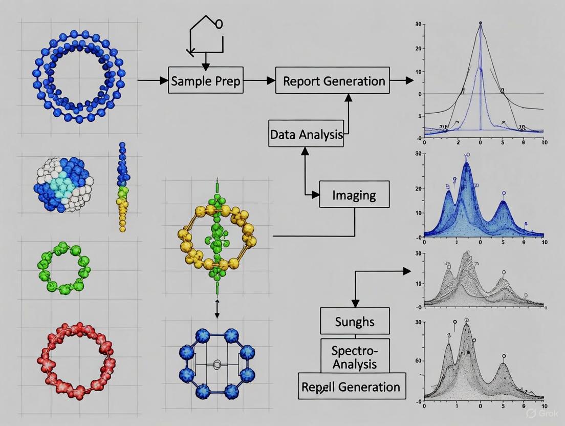
Visualizing AFM Operation and Experimental Workflow
AFM Experimental Workflow
This workflow outlines the standardized procedure for AFM analysis of optical components, from sample preparation through data validation, highlighting key decision points for operational mode selection and critical analysis outputs.
AFM Working Principle
This diagram illustrates the core working principle of atomic force microscopy, showing how laser detection of cantilever deflection combined with precision positioning and feedback control enables nanoscale topography measurement.
Atomic Force Microscopy provides an indispensable toolkit for quantitative surface topography analysis with unmatched vertical resolution. For optical component cleaning validation research, AFM offers the unique capability to directly correlate nanoscale surface changes with macroscopic performance metrics. The precise roughness parameters obtained through standardized AFM protocols—particularly Sa, Sq, skewness, and kurtosis—enable researchers to objectively quantify cleaning effectiveness and its impact on optical performance. As optical technologies continue to demand higher precision, AFM remains a critical validation tool, bridging the gap between nanoscale surface topography and functional optical properties through rigorous, quantitative measurement.
How AFM Directly Assesses Contamination Status and Cleaning Effectiveness
Atomic Force Microscopy (AFM) has emerged as a critical analytical technique for the direct assessment of contamination status and cleaning effectiveness on sensitive surfaces, including optical components. Unlike many other surface analysis techniques, AFM provides non-destructive, three-dimensional imaging with nanoscale resolution under ambient air or liquid conditions, making it uniquely suited for evaluating cleaning protocols without altering the sample surface [24]. This capability is particularly valuable for researchers and drug development professionals who require precise quantification of surface topography changes resulting from contamination and subsequent cleaning procedures. The technology enables direct visualization and quantitative measurement of surface features, allowing for objective comparison of cleaning methods based on empirical data rather than indirect indicators.
AFM operates by scanning a sharp tip attached to a microcantilever across a sample surface, detecting minute forces between the tip and the surface to generate detailed topographical maps [24]. This mechanism allows for the characterization of various surface properties, including morphology, roughness, and adhesion forces, all of which are essential parameters for evaluating cleaning efficacy. For optical components, where even nanometer-scale contaminants can significantly impair performance, AFM provides the necessary resolution to directly assess both contamination presence and removal effectiveness [14] [25].
AFM Methodologies for Contamination Assessment
Surface Topography and Roughness Analysis
The primary application of AFM in cleaning validation involves the detailed measurement of surface topography before and after cleaning procedures. This is typically achieved through high-resolution imaging in either contact or tapping mode, with the latter being particularly suitable for soft, easily deformed, or delicate samples [24]. The quantitative data derived from these scans enables researchers to calculate key parameters that directly reflect contamination status and cleaning effectiveness:
Root Mean Square (RMS) Roughness (δ): This parameter provides a statistical measure of surface height variations, calculated as the standard deviation of height values from the mean plane [25]. The mathematical expression is:
where N represents the number of data points and z_i is the height deviation at each point.
Power Spectral Density (PSD) Function: This function, derived from the Fourier transform of the autocovariance function, offers information about the frequency spectrum of surface roughness and helps distinguish between different types of surface features [25].
Research demonstrates that AFM roughness measurements can reveal how cleaning processes affect surface morphology. One study on fused silica wafers found that a standard cleaning treatment (basic peroxide followed by acidic peroxide) decreased surface roughness by partially removing surface nodules, while also introducing finer features that increased roughness in some measurement parameters [25].
Adhesion Force Measurements
Beyond topographical mapping, AFM can quantify surface adhesion forces using colloidal probe techniques [24]. This application is particularly valuable for understanding the fundamental interactions between contaminants and surfaces. By functionalizing AFM tips with specific contaminant materials or cleaning agents, researchers can measure the force required to separate the tip from the surface, providing direct insight into:
- Contaminant-surface binding strength before and after cleaning treatments
- Residual contamination levels following cleaning procedures
- Effectiveness of different cleaning methods in reducing adhesion forces
This approach allows for a mechanistic understanding of cleaning processes at the nanoscale, complementing the topological data obtained through surface imaging.
Experimental Data on Cleaning Effectiveness
Quantitative Assessment of Cleaning Methods
Recent research has generated substantial quantitative data demonstrating AFM's effectiveness in evaluating various cleaning techniques for sensitive surfaces. The following table summarizes key findings from studies investigating different cleaning methods:
Table 1: AFM Assessment of Cleaning Methods for Various Surfaces
| Surface Type | Cleaning Method | Key AFM Findings | Reference |
|---|---|---|---|
| Optical Components (Fused Silica, Chemical Coating, Multilayer Dielectric Coating) | Low-pressure plasma cleaning | Effectively removed organic contaminants; completely restored performance of optical components | [14] |
| Fused Silica Wafers | Basic peroxide followed by acidic peroxide | Decreased dominant nodule size (100-300 nm to 50-150 nm); reduced RMS roughness from 1.89 nm to 1.36 nm; introduced finer features | [25] |
| AFM Calibration Samples | New Skin technique combined with UV/ozone | Effectively removed large contaminants without mechanical damage; UV/ozone eliminated microscopic organic layers | [26] |
| Silicon Carbide (SiC) Fibers | High-speed AFM assessment | Enabled reliable quantification of surface roughness with minimal uncertainty; distinguished samples with 34-53 nm Sa roughness | [27] |
AFM Roughness Parameters for Cleaning Validation
The application of AFM for quality control in cleaning validation has been enhanced through high-speed AFM (HS-AFM), which enables the collection of statistically powerful measurements through rapid image acquisition [27]. This approach allows researchers to distinguish between similar surfaces based on nanoscale roughness parameters, as demonstrated in studies on silicon carbide fibers where area roughness parameters (Sa) provided more statistically significant data compared to line roughness measurements [27]. The table below outlines key AFM roughness parameters used in cleaning validation:
Table 2: Key AFM Roughness Parameters for Cleaning Assessment
| Parameter | Description | Application in Cleaning Validation |
|---|---|---|
| RMS Roughness (Rq or δ) | Root mean square average of height deviations from the mean plane | Primary indicator of surface smoothness after cleaning |
| Area Roughness (Sa) | Three-dimensional equivalent of Ra (arithmetic average height) | Provides comprehensive assessment of cleaning efficacy across surface area |
| Power Spectral Density (PSD) | Frequency spectrum of surface roughness | Identifies specific spatial wavelength features affected by cleaning |
| Surface Area Ratio | Ratio of measured surface area to geometric area | Quantifies increase in effective area due to roughness; indicates cleaning impact on surface topography |
Experimental Protocols for AFM Assessment
Standardized AFM Imaging Protocol
To ensure consistent and reproducible assessment of cleaning effectiveness, researchers should follow a standardized imaging protocol:
Sample Preparation: Mount cleaned and uncleaned samples on appropriate substrates. Ensure samples are securely fixed to prevent movement during scanning.
AFM Calibration: Calibrate the AFM using reference standards with known dimensions to verify scanner accuracy in x, y, and z directions.
Imaging Parameters:
- Scan Size: Select appropriate areas (typically 1×1 μm to 10×10 μm) to represent both general surface features and specific regions of interest
- Resolution: Use 512×512 or 1024×1024 pixels for adequate detail
- Scan Rate: Adjust (typically 0.5-2 Hz) to optimize image quality and minimize tip wear
- Operating Mode: Choose contact mode for hard surfaces or tapping mode for soft, delicate surfaces [24]
Multiple Area Selection: Image at least three different regions on each sample to account for surface heterogeneity.
Data Acquisition: Collect height, amplitude, and phase data for comprehensive analysis.
Contamination-Specific Assessment Methods
Different types of contamination require specialized assessment approaches:
Organic Contamination Assessment:
- Utilize UV/ozone cleaning as a reference method, as it rapidly decomposes organic contaminants through oxidation [26]
- Combine with AFM imaging to verify removal of hydrocarbon layers
- Safety Note: UV/ozone techniques require proper safety measures as short-wavelength UV and ozone are both hazardous [26]
Particulate Contamination Assessment:
- Apply gentle cleaning methods like the New Skin technique to remove large contaminants without mechanical damage to sensitive surfaces [26]
- Use AFM to verify particulate removal while monitoring for surface scratches or damage
Biomolecular Contamination Assessment:
- Employ AFM in liquid environments to maintain biomolecular integrity [24]
- Use adhesion force mapping with functionalized tips to detect specific biomolecular residues
Comparative Analysis with Alternative Techniques
AFM offers distinct advantages over other surface analysis techniques for cleaning validation, though each method has its appropriate applications. The following diagram illustrates the decision pathway for selecting the appropriate analytical technique:
Decision Pathway for Cleaning Assessment Techniques
Table 3: Comparison of Surface Analysis Techniques for Cleaning Validation
| Technique | Resolution | Environment | Sample Requirements | Key Advantages | Key Limitations |
|---|---|---|---|---|---|
| Atomic Force Microscopy (AFM) | Atomic to nanoscale | Ambient air or liquid | Any solid material | 3D topography, quantitative roughness, works in liquid, measures mechanical properties | Slow scan speed (traditional AFM), small scan area |
| Scanning Electron Microscopy (SEM) | Nanoscale | Vacuum | Conductive (or coated) | Large scan areas, high resolution imaging | Vacuum incompatible with some samples, complex preparation, no 3D data |
| Optical Microscopy | Diffraction-limited (∼200 nm) | Ambient | Any | Fast, easy sample preparation, large area view | Limited resolution, qualitative assessment only |
| High-Speed AFM (HS-AFM) | Nanoscale | Ambient air or liquid | Any solid material | Fast image acquisition, statistical power for QC | Specialized equipment, smaller scan sizes |
As evidenced in the table, AFM provides unique capabilities for cleaning validation, particularly its operation in liquid environments and ability to generate quantitative 3D topographical data without requiring conductive coatings or vacuum conditions [24]. The development of High-Speed AFM (HS-AFM) has addressed traditional limitations in imaging speed, making it suitable for quality control applications where statistical power is essential [27].
Essential Research Reagents and Materials
Successful AFM assessment of cleaning effectiveness requires specific reagents and materials. The following table details essential items for related experiments:
Table 4: Essential Research Reagents and Materials for AFM Cleaning Assessment
| Item | Specification/Type | Function/Application |
|---|---|---|
| AFM Instrument | With tapping/contact mode capabilities | Primary imaging and force measurement |
| AFM Probes | Various stiffnesses for different samples | Surface sensing and imaging |
| UV/Ozone Cleaner | Commercial or custom-built | Removing organic contaminants through oxidation [26] |
| Plasma Cleaning System | Low-pressure plasma | Removing organic contamination from sensitive optical components [14] |
| Chemical Cleaners | Basic peroxide (NH₄OH:H₂O₂:H₂O 1:1:5) | Removing organic contaminants and activating surfaces [25] |
| Chemical Cleaners | Acidic peroxide (HCl:H₂O₂:H₂O 1:1:5) | Removing metallic ions and further cleaning [25] |
| Reference Samples | Certified roughness standards | AFM calibration and verification |
| Sample Mounting Supplies | Double-sided tape, magnetic disks | Secure sample placement during scanning |
AFM provides researchers and drug development professionals with a powerful, direct method for assessing contamination status and cleaning effectiveness on optical components and other critical surfaces. Through quantitative measurement of surface topography, roughness parameters, and adhesion forces, AFM enables objective comparison of cleaning methods based on empirical data at the nanoscale. The technique's unique capability to operate in liquid environments and analyze both conductive and non-conductive materials without destructive sample preparation makes it particularly valuable for validating cleaning protocols for sensitive optical components used in pharmaceutical research and development.
As AFM technology continues to advance, particularly with the development of high-speed systems and enhanced probe designs, its application in cleaning validation is expected to expand, providing even more precise and statistically robust assessment of cleaning efficacy for optical components in research and drug development applications.
Atomic force microscopy (AFM) serves as a critical tool for validating the efficacy of cleaning processes for optical components. The presence of organic contamination and surface defects on optics such as uncoated fused silica, chemical coatings, and multilayer dielectric coatings can severely compromise performance in high-power laser systems, leading to reduced transmission and lowered laser-induced damage threshold (LIDT) [14]. This case study objectively compares the surface characteristics of these three optical components before and after low-pressure plasma cleaning through AFM analysis. We present quantitative AFM data, detailed experimental protocols, and analytical workflows to provide researchers with a validated framework for assessing cleaning effectiveness and surface integrity. The findings demonstrate AFM's indispensable role in optical component lifecycle management, from initial fabrication to in-service maintenance and performance validation.
Experimental Protocols and Methodologies
Sample Preparation and Characterization
The study investigated three representative optical components: uncoated fused silica substrates, chemical-coated optics, and multilayer dielectric-coated optics [14]. Prior to cleaning, all samples underwent controlled contamination to simulate field conditions. The cleaning process utilized low-pressure plasma generation systems with optimized parameters for organic contaminant removal. Pre- and post-cleaning characterization employed multiple complementary techniques: water contact angle measurements provided indirect assessment of surface cleanliness and energy, while spectrophotometry evaluated optical performance through transmission and reflection metrics [14]. Laser-induced damage threshold testing quantified the functional performance recovery after cleaning.
AFM Imaging and Analysis Parameters
AFM measurements were performed using a Dimension Icon AFM (Bruker) operating in tapping mode to minimize surface damage [28]. Standard silicon probes with resonant frequencies of approximately 300 kHz and nominal tip radii of 5-10 nm ensured high-resolution topography mapping. Multiple scan areas from (1×1) μm² to (50×50) μm² captured both nanoscale features and microscale surface trends. For each sample condition, at least three different locations were scanned to ensure statistical significance. The resulting topography images were processed and analyzed using Gwyddion open-source software, which enabled calculation of root-mean-square (RMS) roughness (Sq), power spectral density (PSD) functions, and defect density quantification [28].
Table 1: Key Research Reagent Solutions for AFM Analysis of Optical Components
| Reagent/Material | Function in Research | Application Context |
|---|---|---|
| Fused Silica Substrates | Reference substrate material | Baseline surface for contamination/cleaning studies |
| Ethanol & Acetone | Solvent cleaning agents | Initial substrate preparation [29] |
| Argon Plasma | Surface activation & cleaning | In-situ vacuum chamber cleaning pre-deposition [29] |
| Xanthine Organic Layer | Nanostructure template material | Forms self-organizing structures for AR coatings [28] |
| O₂/Ar Gas Mixture | Plasma etching chemistry | Creates nanostructures from organic layers [28] |
| SiO₂ & TiO₂ Pellets | Coating source materials | Electron beam evaporation for optical coatings [29] |
Contamination and Cleaning Simulation
To standardize testing, organic contaminants representative of those found in laser system environments were artificially applied to all three optical component types. The low-pressure plasma cleaning process was then applied with precisely controlled parameters including gas composition, pressure, power, and treatment duration. This systematic approach enabled direct comparison of cleaning effectiveness across different coating types and established optimal cleaning parameters for each material system while minimizing substrate damage.
Results and Comparative Analysis
Quantitative AFM Surface Topography Data
AFM analysis provided quantitative measurement of surface roughness and nanostructural evolution before and after plasma cleaning. The data revealed distinct responses to cleaning processes across the three optical component types, reflecting their different material compositions and surface properties.
Table 2: AFM Roughness Analysis Across Optical Component Types
| Optical Component Type | Pre-Cleaning RMS Roughness (nm) | Post-Cleaning RMS Roughness (nm) | Roughness Change | Key Surface Features Identified |
|---|---|---|---|---|
| Uncoated Fused Silica | 0.35 ± 0.05 | 0.38 ± 0.06 | Minimal increase | Isolated nanopits, minimal scratching |
| Chemical Coating | 1.82 ± 0.15 | 1.85 ± 0.14 | Minimal increase | Dense granular morphology, uniform texture |
| Multilayer Dielectric Coating | 0.71 ± 0.09 | 0.73 ± 0.08 | Minimal increase | Columnar microstructure, interface defects |
The near-identical RMS roughness values before and after plasma cleaning across all sample types indicate that the cleaning process effectively removed contaminants without significantly altering the intrinsic surface topography. This preservation of original surface structure is critical for maintaining the designed optical performance of precision components.
Power Spectral Density Analysis
AFM-based power spectral density analysis quantified surface structure across spatial frequency ranges from 0.02 μm⁻¹ to 256 μm⁻¹, corresponding to feature sizes from approximately 4 nm to 50 μm [28]. This multi-scale analysis revealed that the plasma cleaning process did not introduce periodic structures or alter the characteristic lateral distribution of surface features across all three optical component types. The PSD curves maintained nearly identical slopes and magnitudes before and after cleaning, confirming the non-abrasive nature of the plasma cleaning process.
Correlation with Functional Performance Metrics
Water contact angle measurements demonstrated significant changes after plasma cleaning, with all three optical component types showing substantial reductions in contact angles, indicating increased surface energy and complete removal of organic contaminants [14]. This surface cleaning translated directly to functional performance recovery, with spectrophotometry confirming restored transmission characteristics and laser-induced damage threshold testing demonstrating complete recovery to baseline LIDT values [14]. The AFM analysis provided the critical surface structural evidence explaining this performance recovery by confirming the absence of permanent surface damage that could serve as damage precursors under high-power laser operation.
Discussion
AFM as a Validation Tool for Cleaning Processes
This comparative study demonstrates AFM's critical role in validating optical component cleaning processes. The quantitative topography data confirmed that low-pressure plasma cleaning effectively removed organic contaminants without introducing additional surface defects that could act as laser damage precursors [14]. The power spectral density analysis provided comprehensive characterization of surface structures across spatial frequencies, offering insights beyond simple roughness measurements. For uncoated fused silica, AFM verified the preservation of pristine surface conditions post-cleaning. With chemical coatings, AFM confirmed maintenance of granular morphology essential for optical performance. For multilayer dielectric coatings, AFM monitoring ensured the complex layered structure remained intact through the cleaning process, particularly at vulnerable interfaces between materials with different chemical and mechanical properties [30].
Implications for Laser Damage Threshold
The AFM findings directly correlate with enhanced laser damage resistance. Surface defects identified through AFM, including scratches, pits, and particulate contamination, function as field enhancement centers that lower LIDT [30]. The demonstration that plasma cleaning removes contaminants without adding new defects provides a scientific basis for the observed LIDT recovery [14]. This is particularly crucial for multilayer dielectric coatings where interfacial defects and columnar microstructure can dominate damage initiation [30]. AFM enables researchers to differentiate between intrinsic coating defects and process-induced contaminants, guiding targeted improvements in both coating fabrication and maintenance cleaning protocols.
Comparative Advantages of AFM Analysis
AFM provides distinct advantages over other characterization techniques for cleaning validation. Unlike light scattering techniques that offer only indirect assessment, AFM delivers direct three-dimensional topography with nanometer-scale resolution. Compared to electron microscopy, AFM requires no conductive coatings that could alter surface properties, and can be performed under ambient conditions rather than high vacuum. The ability to combine quantitative roughness measurements with defect identification and surface structure analysis makes AFM uniquely capable of comprehensive cleaning validation. Furthermore, AFM's compatibility with transparent optical materials without special preparation enables direct analysis of operational components.
This systematic case study demonstrates that AFM analysis provides critical quantitative data for validating cleaning processes across three fundamental optical component types. The results confirm that low-pressure plasma cleaning effectively removes organic contaminants from uncoated fused silica, chemical coatings, and multilayer dielectric coatings without significantly altering intrinsic surface topography. AFM measurements revealed negligible changes in RMS roughness following cleaning, with values remaining at 0.38 nm for fused silica, 1.85 nm for chemical coatings, and 0.73 nm for multilayer dielectric coatings. Power spectral density analysis further confirmed the preservation of original surface characteristics across spatial frequencies. These findings validate AFM as an essential tool for optical component lifecycle management, enabling researchers and engineers to verify cleaning efficacy, predict laser damage threshold behavior, and maintain optimal performance in high-power laser systems. The experimental protocols and analytical frameworks presented provide a standardized methodology for future comparative studies of optical surface treatments and cleaning technologies.
A Practical AFM Methodology for Cleaning Validation Protocols
Integrating AFM into a Risk-Based Cleaning Validation Lifecycle Approach
In the highly regulated pharmaceutical and advanced manufacturing industries, cleaning validation is paramount for preventing cross-contamination and ensuring product safety. Traditional cleaning validation protocols, while effective, often rely on methods that provide limited data on the nanoscale residues that can compromise product quality. A risk-based lifecycle approach emphasizes proactive and scientifically sound methods to control contamination throughout a product's lifecycle. Within this framework, Atomic Force Microscopy (AFM) is emerging as a powerful tool that provides nanoscale resolution for detecting and characterizing residues that other methods cannot. This guide compares the performance of AFM with traditional analytical techniques, providing a clear rationale for its integration into modern cleaning validation strategies.
AFM, invented in 1986, is a versatile scanning probe technique that achieves nanoscale resolution by measuring the forces between a sharp tip and a sample surface [31] [24]. Its key advantage lies in its ability to perform in-situ 3D imaging and quantitative mechanical property measurements under ambient or liquid conditions, without requiring complex sample preparation or conductive coatings [24]. This makes it uniquely suitable for analyzing sensitive surfaces, such as pharmaceutical manufacturing equipment or optical components, in their native state.
Comparative Analysis: AFM vs. Traditional Cleaning Validation Techniques
The following table summarizes the core capabilities of AFM against traditional methods used in cleaning validation, such as Total Organic Carbon (TOC) analysis and High-Performance Liquid Chromatography (HPLC).
Table 1: Performance Comparison of Cleaning Validation and Surface Analysis Techniques
| Technique | Primary Function | Detection Sensitivity | Key Measurable Parameters | Sample Requirements & Conditions |
|---|---|---|---|---|
| Atomic Force Microscopy (AFM) | Surface topography imaging & nanomechanical characterization | Sub-nanometer vertical resolution [31] | Morphology, roughness, adhesion forces, elastic modulus [24] [32] | Ambient air or liquid; no special preparation [24] |
| Total Organic Carbon (TOC) | Bulk residue quantification | Parts-per-billion (ppb) for carbon [33] | Total organic carbon content [33] | Requires soluble residues; rinse water or swab extract |
| High-Performance Liquid Chromatography (HPLC) | Specific compound identification & quantification | Parts-per-million (ppm) for specific analytes [33] | Concentration of a specific active ingredient or residue [34] | Requires method development; destructive testing |
| Swab Sampling + Analytical Method | Surface residue recovery and quantification | Technique-dependent (e.g., ppm with HPLC) [34] | Mass of residue recovered from a defined area [35] [34] | Invasive; recovery efficiency varies; technique-dependent results [34] |
Key Performance Differentiators
- Spatial Resolution vs. Bulk Analysis: While TOC and HPLC provide excellent sensitivity for quantifying the amount of residue present, they offer no information on its spatial distribution or physical nature on the surface [33] [34]. AFM uniquely maps the nanoscale topography and morphology of residues, identifying thin films, particulate contaminants, and crystallized deposits that can evade bulk analytical methods [24].
- Functional Property Measurement: Beyond visualization, AFM can measure adhesion forces and nanomechanical properties (e.g., stiffness, elasticity) using techniques like force spectroscopy [24] [32]. This allows researchers to understand not just if a residue is present, but how strongly it adheres to the surface and its mechanical behavior, which directly impacts cleaning effectiveness.
- The Complementarity of Techniques: AFM is not a replacement for established techniques like TOC but a powerful complement. A risk-based strategy might use TOC for rapid, routine verification of cleaning effectiveness while deploying AFM for root-cause investigation of validation failures or to study the fundamental mechanisms of residue adhesion and removal during process development [33].
Experimental Protocols for AFM in Cleaning Validation
Integrating AFM into a cleaning validation protocol requires a structured methodology to ensure reproducible and meaningful data. The following workflow outlines a standardized approach, from sample preparation to data analysis.
Diagram 1: AFM Integration Workflow
Sample Preparation and Contamination
The first step involves creating representative test samples. A risk-based approach often employs a "worst-case scenario" using an Active Pharmaceutical Ingredient (API) with poor solubility and high cleaning difficulty [35].
- API Selection: Select a challenging compound, such as Oxcarbazepine, which is sparingly soluble in water (0.07 mg/mL), making it difficult to remove [35].
- Surface Soiling: Contaminate a defined area (e.g., a 100 cm² section of stainless steel, a material common in pharmaceutical equipment) with a known quantity of the API [35].
- Drying Process: Allow the contaminant to dry under controlled conditions to simulate process-related residue.
AFM Measurement Execution
- Cantilever Selection and Calibration: For imaging cleaned surfaces, standard silicon cantilevers with a nominal tip radius of <10 nm and resonant frequencies of 306-353 kHz are suitable [32]. For quantitative force measurements, cantilevers must be calibrated for their spring constant. This can be done using thermal tune methods or, for higher accuracy, with certified reference cantilevers like NIST SRM 3461 [36].
- Measurement Modes:
- Tapping Mode: Used for high-resolution topographic imaging of surfaces and residues with minimal damage. This mode can distinguish different material phases via phase imaging [31] [24].
- Force Spectroscopy: The AFM tip is approached and retracted from the surface to obtain a force-distance curve. This quantifies the adhesion force between the tip and the surface, which is a direct measure of residue stickiness [24] [37].
Data Analysis and Risk Assessment
- Topography and Roughness: Analyze AFM height images to calculate surface roughness parameters (e.g., Ra, Rq). An increase in roughness after cleaning may indicate residue or surface damage [32].
- Adhesion Force Mapping: Collect force curves at multiple points to create an adhesion force map. Consistently high adhesion forces across a "cleaned" surface indicate the presence of residual contaminant films [24] [37].
- Setting Action Limits: Establish acceptable thresholds for surface roughness and adhesion force based on correlation with other analytical methods (e.g., TOC) or historical validation data. Surfaces exceeding these limits trigger a corrective action within the quality system.
The Scientist's Toolkit: Essential Reagents and Materials
Table 2: Key Research Reagent Solutions for AFM-Based Cleaning Validation
| Item | Function/Description | Application Context |
|---|---|---|
| NIST SRM 3461 | Standard Reference Material for AFM cantilever spring constant calibration [36]. | Ensures quantitative and metrologically traceable force measurements, critical for reproducible data across labs. |
| Standard Silicon Cantilevers | Probes with sharp tips (radius <10 nm) for high-resolution imaging [32]. | General topography imaging of surfaces and particulate residues. |
| Colloidal Probe Cantilevers | Cantilevers with a microsphere attached to the end [24]. | Measures interaction forces with defined geometry, simulating the adhesion of a spherical contaminant or cell. |
| Polyester Swabs | Absorbent material for traditional swab sampling [35]. | Used for comparative analysis: swab sampling of a defined area followed by HPLC/TOC analysis vs. AFM surface mapping. |
| Analytical Solvents (e.g., Acetonitrile) | High-purity solvents for dissolving residues [35]. | Used in recovery studies to optimize sampling methods and as a diluent for analytical techniques like HPLC. |
The integration of AFM into a risk-based cleaning validation lifecycle represents a significant advancement in quality assurance. While traditional methods like TOC and HPLC remain essential for quantifying specific residues, AFM provides an unmatched capability to visualize, measure, and understand contamination at the nanoscale. Its ability to perform in-situ analysis and measure functional properties like adhesion force makes it an indispensable tool for root-cause analysis, process optimization, and building a more robust scientific case for cleaning process validation. As regulatory expectations evolve towards a more knowledge-driven, lifecycle approach, AFM is poised to become a critical technology for ensuring the highest standards of product quality and safety in pharmaceuticals and advanced manufacturing.
Atomic force microscopy (AFM) is an indispensable tool in nanotechnology and materials science, enabling high-resolution 3D topography visualization and nanomechanical characterization of a wide range of samples [38]. The technique operates by scanning a sharp probe mounted on a flexible cantilever across a sample surface, measuring interactions between the tip and sample to generate detailed images [39] [40]. Unlike electron microscopy, AFM can perform these measurements in ambient air or liquid environments without requiring conductive coatings or vacuum conditions, making it particularly valuable for analyzing soft, biological, or insulating materials [38] [40].
The quality of AFM data is profoundly influenced by sample preparation, which serves as the critical foundation for reliable analysis. Proper preparation techniques ensure that samples are rigidly adhered, appropriately dispersed, and structurally preserved, enabling accurate measurement of surface properties and nanomechanical characteristics [38]. This guide systematically compares the three principal preparation methodologies—swabbing, rinsing, and mounting—within the specific context of validating cleaning processes for optical components, a crucial application in maintaining the performance of high-precision laser systems [14].
Core Sample Preparation Methodologies
AFM sample preparation encompasses all procedures required to present a representative region of interest to the AFM probe in a stable, uncontaminated state. For optical component analysis, the primary goals include removing particulate and organic contaminants, preserving native surface structures, and ensuring secure fixation to prevent drift during scanning. The following sections objectively compare the three central techniques.
Swabbing
Swabbing involves the mechanical application of cleaning solutions or collection of contaminants from surfaces using fibrous tips. While not extensively detailed in the available AFM protocols for biological tissues, the principle of mechanical action is implied in contamination removal studies.
- Mechanism: Mechanical abrasion and adsorption onto swab material.
- Typical Applications: Pre-cleaning of optical components before detailed analysis [14], collection of surface contaminants for off-site analysis.
- Experimental Data: Research on optical components indicates that organic contamination gradually impairs performance by increasing scatter and reducing laser-induced damage threshold [14]. Swabbing represents an initial step in addressing this contamination.
- Limitations: Risk of leaving residual fibers, potential for scratching sensitive surfaces, and difficulty in standardizing applied pressure.
Rinsing
Rinsing employs solvents to remove loosely bound contaminants, salts, or residual reagents from sample surfaces. This method is particularly critical for preparing biological specimens and for final cleaning steps of optical components.
- Mechanism: Solvation and hydrodynamic removal of contaminants.
- Protocol Details: In retinal capillary isolation for AFM stiffness measurements, extensive rinsing sequences are employed [41]. The protocol specifies:
- Transferring a fixed retina through six sequential wells of double-distilled H₂O.
- Rinsing on an orbital shaker at 120 RPM for 30 minutes per well at room temperature.
- Gentle agitation by pipetting water adjacent to the sample between transfers.
- A final overnight rinse at 100 RPM to facilitate separation of retinal neuroglia from blood vessels [41].
- Experimental Data: For optical components, low-pressure plasma cleaning effectively removes organic contaminants that rinsing alone may not address, completely restoring component performance as validated by AFM and transmittance measurements [14].
- Limitations: May not remove strongly adhered contaminants; requires optimization of solvent composition, volume, and duration to prevent sample alteration or re-deposition of contaminants.
Mounting
Mounting encompasses securing the sample to a substrate rigid enough to prevent drift during AFM scanning while ensuring optimal surface exposure. This is the most extensively documented preparation step in AFM literature.
- Mechanism: Physical adhesion or chemical bonding to a substrate.
- Protocol Details: Successful mounting requires careful selection of substrates and adhesives based on sample properties:
- Substrate Selection: Smaller nanomaterials require smoother substrates. Mica provides an atomically flat surface after cleavage and is ideal for high-resolution imaging. Silicon and glass offer good flatness for larger nanoparticles, while metal discs suit larger particles [38].
- Adhesion Activation: Electrostatic or chemical bonding is often enhanced by adhesives. Poly-L-lysine (PLL) works well with mica, while 3-aminopropyldimethylethoxysilane (APDMES) is suitable for silicon substrates [38]. The adhesive affinity for the sample must exceed that between the sample and the AFM tip to prevent pick-up.
- Incubation and Drying: Samples are incubated with the substrate for duration dependent on particle size, then rinsed with deionized water and dried with nitrogen gas before visualization [38].
- Experimental Data: An optimized drop-casting protocol for graphene nanosheets uses a mixed solvent of EtOH/H₂O (volume ratio 2:8) and a pre-heated (150°C) silicon wafer with a 300 nm oxide layer to achieve uniform distribution, minimal stacking, and proper density for high-throughput AFM analysis [42].
- Limitations: Substrate roughness can interfere with fine feature visualization; inadequate adhesion causes sample displacement during scanning; over-fixation can alter sample properties.
Comparative Analysis of Preparation Methods
The table below provides a systematic comparison of the three preparation methodologies based on effectiveness, applications, and limitations.
Table 1: Comparative Analysis of AFM Sample Preparation Methods
| Method | Effectiveness | Typical Applications | Key Limitations |
|---|---|---|---|
| Swabbing | Moderate for particulate removal | Initial cleaning of optical components [14] | Risk of surface damage, fiber residue, variable effectiveness |
| Rinsing | High for soluble contaminants | Biological tissue preparation [41], final cleaning steps | Less effective for adhered contaminants, solvent compatibility issues |
| Mounting | Essential for stable imaging | Universal requirement for AFM analysis [38] | Substrate roughness interference, adhesion challenges |
Performance Data in Optical Component Validation
In studies validating optical component cleaning, AFM serves as a direct assessment tool for surface contamination and cleaning effectiveness [14]. Research on fused silica and coated optics demonstrates that:
- Contamination Impact: Organic contaminants significantly increase surface roughness measured by AFM and impair transmittance and laser-induced damage threshold.
- Cleaning Validation: Low-pressure plasma cleaning effectively removes contaminants, with AFM topography showing restored surface morphology and corresponding recovery of optical performance [14].
- Method Integration: A combined approach using rinsing for initial contaminant removal followed by plasma treatment and AFM validation provides comprehensive cleaning assessment.
Table 2: AFM in Cleaning Validation for Optical Components
| Component Type | Contamination Effect | AFM Validation Metric | Post-Cleaning Result |
|---|---|---|---|
| Uncoated Fused Silica | Increased surface roughness | Nanoscale topography | Complete performance restoration [14] |
| Chemical Coating | Organic contaminant adsorption | Adhesion force, roughness | Recovered transmittance [14] |
| Multilayer Dielectric Coating | Performance deterioration | Laser-induced damage threshold | Restored surface properties [14] |
The Scientist's Toolkit: Essential Research Reagents and Materials
The following table details essential materials required for implementing the sample preparation protocols discussed, particularly for mounting procedures.
Table 3: Essential Materials for AFM Sample Preparation
| Item | Function/Application | Specific Examples |
|---|---|---|
| AFM Substrates | Provides flat, stable surface for sample analysis | Mica discs (cleaved fresh), silicon wafers, glass slides, metal discs [38] |
| Adhesives | Promotes sample fixation to substrate | Poly-L-lysine (for mica), 3-aminopropyldimethylethoxysilane (for silicon) [38] |
| Cleaning Solvents | Removes contaminants and residual adhesives | Double-distilled water, ethanol, isopropanol [41] [42] |
| Sample Materials | Target specimens for analysis | Isolated mouse retinal capillaries [41], graphene nanosheets [42], optical components [14] |
Integrated Workflow for AFM Sample Preparation
The following workflow diagram integrates multiple preparation methods into a coherent process for optical component analysis, synthesized from the reviewed protocols.
Diagram 1: Integrated AFM sample preparation workflow for optical components.
Swabbing, rinsing, and mounting each fulfill distinct yet complementary roles in the AFM sample preparation pipeline for optical component analysis. Swabbing provides initial contaminant reduction, rinsing effectively removes soluble contaminants and preparation artifacts, while mounting creates the essential stable interface for high-resolution imaging. The optimal preparation strategy typically integrates these methods sequentially, with specific protocols tailored to sample properties and analytical objectives. AFM subsequently serves as the critical validation tool, directly quantifying surface topography and nanomechanical properties to verify cleaning efficacy and component integrity [14]. As AFM technology continues advancing with improved automation and AI-driven analysis [39], standardized preparation methodologies will become increasingly vital for generating reproducible, reliable data in optical component research and across nanotechnology applications.
Atomic force microscopy (AFM) enables nanoscale characterization of surface properties, making it indispensable for validating the cleanliness and integrity of optical components. This guide provides a detailed operational protocol for obtaining reproducible AFM measurements, focusing on the critical decisions from probe selection to final image acquisition. We objectively compare probe performance and operational modes using experimental data to guide researchers in optimizing their AFM methodology for sensitive applications like cleaning validation, where nanoscale contaminants can compromise optical system performance.
AFM Probe Selection and Comparison
The selection of an appropriate AFM probe is the most critical parameter determining measurement quality. Probes must be matched to specific application requirements including imaging mode, sample properties, and environmental conditions [43].
Probe Characteristics and Specifications
- Tip Geometry: Tip sharpness, defined by apex radius and cone angle, directly determines spatial resolution. High-aspect-ratio tips are essential for probing deep or confined nanostructures [13] [43].
- Cantilever Properties: Spring constant and resonant frequency dictate force sensitivity and imaging speed. Stiffer cantilevers (higher spring constants) are suitable for hard materials, while softer cantilevers prevent sample damage on delicate surfaces [13] [43].
- Material Composition: Silicon (Si) probes offer excellent sharpness and balanced mechanical properties. Silicon nitride (Si₃N₄) provides enhanced durability, while diamond-coated tips offer extreme wear resistance for abrasive samples [13] [43].
- Specialized Functionalizations: Conductive coatings enable electrical measurements, while functionalized probes with specific chemical groups or biomolecules allow chemical mapping and biological sensing [43].
Quantitative Probe Performance Comparison
Table 1: Comparative Performance of AFM Probes for Different Applications
| Probe Type | Apex Radius (nm) | Half-Cone Angle | Spring Constant | Best For | Limitations |
|---|---|---|---|---|---|
| Standard Si (NanoWorld) | ~10 | 30°-70° [13] | Varies by model | General topography, moderate resolution | Limited aspect ratio, blunter angles [13] |
| Ultra-Sharp HAR Si | 5 [13] | 7.5° [13] | ~19.64 N/m (designed) [13] | High-resolution imaging, deep nanoscale features | Fabrication complexity, higher cost [13] |
| Silicon Nitride (Si₃N₄) | >20 | >35° | Soft (e.g., ~0.1 N/m) | Biological samples, force spectroscopy | Less sharp, lower resolution [13] |
| Carbon Nanotube (CNT) | Exceptional sharpness | Very small | Depends on attachment | Extreme resolution, deep trenches | Poor reproducibility, alignment challenges [13] |
Recent advances in batch fabrication have produced ultra-sharp silicon probes with tip apex radii of approximately 5 nm and half-cone angles of 7.5°, enabling high-resolution and high-fidelity imaging [13]. These probes incorporate stair-shaped handles for universal compatibility with commercial AFM platforms and demonstrate stable scanning performance for up to 8 hours within 100 nm precision range [13].
Step-by-Step AFM Operational Protocol
Stage 1: Pre-Experimental Planning and Probe Selection
Step 1: Define Measurement Objectives
- Identify primary data requirements: topographical mapping, nanomechanical properties, or electrical characterization.
- Determine required resolution and scan size based on feature sizes of interest.
Step 2: Select Appropriate AFM Mode
- Intermittent Contact Mode: Minimizes lateral forces, ideal for weakly adsorbed samples [12].
- Force Spectroscopy: Provides quantitative mechanical properties via force-distance curves [12] [44].
- Nanomechanical Imaging: Maps spatial variations in material properties [12].
- Force Modulation: Differentiates materials based on stiffness variations [12].
Step 3: Probe Selection and Mounting
- Select probe based on Table 1 comparisons and application needs.
- Handle probes with clean tweezers to avoid contamination.
- Mount probe securely in holder, ensuring proper orientation.
Stage 2: System Setup and Calibration
Step 4: Cantilever Calibration
- Calibrate spring constant using thermal tune or reference sample methods [43].
- Determine optical lever sensitivity by measuring cantilever deflection on a rigid sample.
- Verify tip sharpness and cleanliness under optical microscope.
Step 5: Sample Preparation and Mounting
- Clean sample surface appropriately for optical components (solvent cleaning, plasma treatment).
- Securely mount sample on AFM stage using appropriate adhesives or holders.
- Ensure sample is level to minimize tilt in resulting images.
Step 6: Laser Alignment and Detector Setup
- Align laser spot on cantilever back for maximum reflection.
- Center position sensitive detector (PSD) signals.
- Optimize detector sum for stable deflection reading.
Stage 3: Engagement and Scanning Optimization
Step 7: Initial Approach
- Approach tip slowly to surface while monitoring deflection.
- Set appropriate engage parameters to prevent crash.
- Pause approach immediately upon surface detection.
Step 8: Feedback Parameter Optimization
- Setpoint: Adjust to maintain consistent tip-sample interaction.
- Gains: Optimize proportional and integral gains for stable tracking.
- Scan Rate: Balance between imaging speed and tracking fidelity.
Step 9: Image Acquisition
- Start with small scan size to optimize parameters.
- Gradually increase to target scan size while monitoring image quality.
- Acquire multiple scans at different areas for representative sampling.
Stage 4: Data Acquisition and Analysis
Step 10: Data Collection
- Acquire images with sufficient resolution for analysis needs.
- Collect complementary data channels (height, amplitude, phase).
- Document all acquisition parameters for reproducibility.
Step 11: Image Processing
- Apply minimal necessary flattening to remove tilt and bow.
- Use appropriate filtering to enhance features without introducing artifacts.
- Conduct quantitative analysis using validated algorithms.
The workflow for this operational protocol is systematized below:
Comparison of AFM Operational Modes
Different AFM operational modes provide complementary information about sample properties. The selection depends on the specific characterization requirements.
Table 2: Performance Comparison of AFM Operational Modes
| AFM Mode | Resolution | Information Obtained | Best For | Throughput | Sample Considerations |
|---|---|---|---|---|---|
| Intermittent Contact | High | Topography, phase contrast | Delicate samples, rough surfaces | High | Minimal sample damage [12] |
| Force Spectroscopy | Single point | Mechanical properties, adhesion | Quantitative modulus, binding forces | Low | Requires multiple measurements [12] [44] |
| Force Volume | Medium | Spatially resolved mechanical maps | Heterogeneous materials | Low-Medium | Viscoelastic samples [44] |
| Nanomechanical Imaging | High | Simultaneous topography and property maps | Polymer blends, biological cells | Medium | Complex data interpretation [12] |
Advanced nanomechanical mapping modes like force volume, nano-DMA, and parametric methods enable comprehensive characterization of mechanical properties at the nanoscale [44]. These techniques are particularly valuable for optical component cleaning validation, where contaminant mechanical properties differ from substrate materials.
Essential Research Reagent Solutions
Table 3: Key Materials and Reagents for AFM Operation
| Item | Function/Purpose | Application Notes |
|---|---|---|
| Silicon AFM Probes | High-resolution topographical imaging | Select appropriate stiffness based on sample [13] [43] |
| Functionalized Probes | Chemical recognition, specific binding | Modified with chemical groups or biomolecules [43] |
| Reference Samples | Probe calibration, system verification | Grids with known feature sizes for validation |
| Cleaning Solvents | Sample and probe decontamination | Isopropanol, acetone for removing organic residues |
| Adhesive Tape/Mounts | Sample fixation to AFM stage | Double-sided tape, magnetic holders for stability |
| Calibration Gratings | System performance verification | Features with known height and periodicity |
Advanced Applications in Optical Component Validation
AFM provides critical nanoscale validation for optical component cleaning processes through multiple characterization approaches:
- Nanoparticle Contamination Mapping: Ultra-sharp high-aspect-ratio probes detect and quantify residual nanoparticles from cleaning processes with sub-10 nm resolution [13].
- Surface Roughness Quantification: Differentiates between inherent substrate roughness and particulate contamination, essential for laser-induced damage threshold assessment [45].
- Mechanical Property Differentiation: Identifies contaminant materials based on nanomechanical properties, distinguishing between organic residues, metallic particles, and substrate materials [44].
- 3D Surface Characterization: Advanced imaging modes generate three-dimensional topographical data for complete surface characterization [46].
Emerging AFM technologies continue to enhance optical component validation. Localization AFM (LAFM) techniques break resolution limitations set by tip convolution, while new file formats (.afm) enable better data sharing and comparison with other structural biology techniques [47]. Artificial intelligence integration improves data analysis efficiency, with AI-based classifiers demonstrating capability to differentiate between surface types based on nanomechanical properties [45].
For optical component cleaning validation, the combination of high-resolution topographical imaging with nanomechanical property mapping provides the most comprehensive assessment of cleaning efficacy, detecting both particulate contamination and molecular-scale films that can compromise optical performance.
Within optical component cleaning validation research, the precise characterization of surfaces at the nanoscale is paramount. Atomic Force Microscopy (AFM) has emerged as a critical tool for this purpose, enabling researchers to quantitatively assess cleaning efficacy by measuring minute changes in surface topography, residual particle count, and material morphology. This guide provides an objective comparison of AFM performance against alternative techniques and details the experimental protocols for its application in cleaning validation, providing a framework for ensuring the utmost cleanliness and functionality of sensitive optical components.
AFM vs. Alternative Measurement Techniques
The selection of an appropriate metrology technique is fundamental to accurate cleaning validation. The table below provides a structured comparison of AFM with other common surface characterization methods.
Table 1: Comparison of Surface Roughness and Particle Analysis Techniques
| Technique | Principle | Lateral Resolution | Vertical Resolution | Roughness Parameters | Key Advantages | Key Limitations |
|---|---|---|---|---|---|---|
| Atomic Force Microscopy (AFM) [48] [49] | Physical probe scanning surface | <1 nm (probe-dependent) | Angstrom-level [50] | Sa, Sq, Ssk, Sku (3D areal) [49] | Unmatched 3D resolution; works on any solid sample; provides particle height data [48] [51] | Limited scan area; can be slower; requires careful sample prep |
| Stylus Profilometry [52] | Physical stylus tracing surface | Micrometer-scale [48] | Nanometer-scale | Ra, Rq (2D line) | Simple, cost-effective; standardized methods [52] | Low lateral resolution; potential for surface damage; only 2D profile data [48] |
| Optical Profilometry [52] [49] | Optical interferometry | ~200-300 nm (diffraction-limited) [48] | Sub-nanometer | Sa, Sq (3D areal) | Fast, non-contact; good for large areas | Low lateral resolution; transparent samples can pose challenges [48] |
| Scanning Electron Microscopy (SEM) [48] | Focused electron beam | <1 nm | N/A (2D projection) | Cannot directly measure roughness; qualitative assessment only [48] | Excellent top-down imaging and particle counting | Requires conductive coating; no direct height measurement; complex sample environment |
For cleaning validation, the choice of technique hinges on the required sensitivity. While optical and stylus profilers are suitable for larger-scale defects, AFM is the unequivocal tool of choice for quantifying nanoscale roughness and detecting sub-micrometer particulate residue that could compromise optical performance [52] [49]. Its ability to provide three-dimensional, angstrom-resolution data makes it indispensable for verifying ultra-cleaning processes.
Experimental Data from AFM Analysis
AFM generates quantitative data that can statistically validate cleaning protocols. The following table summarizes typical results from different experimental scenarios relevant to cleaning and surface treatment.
Table 2: Experimental AFM Data for Surface and Particle Characterization
| Sample / Treatment Type | Average Roughness (Sa) | RMS Roughness (Sq) | Particle Size / Count | Key Morphological Observations | Source / Context |
|---|---|---|---|---|---|
| Lithium Disilicate Ceramic (Control) [53] | Not Specified (Ra = ~10-20 nm) | Not Specified | N/A | Baseline surface texture | Material baseline characterization |
| Ceramic after Tribochemical Treatment [53] | Not Specified (Ra = ~270-280 nm) | Not Specified | N/A | Significant surface roughening | Effect of aggressive surface treatment |
| Commercial AFM Service (Example) [50] | 0.21 µm | 0.28 µm | N/A | Maximum peak-to-valley (Sz): 1.48 µm | Typical industrial surface measurement |
| NIST Gold Nanoparticles [51] | N/A (assumed smooth substrate) | N/A | 10 nm, 30 nm, 60 nm | Spherical morphology; size confirmed via height measurement | Nanoparticle size and count calibration |
| A. baumannii (Susceptible) [54] | 7.05 nm (cell surface) | Not Specified | Cell size: 1.65 µm by 0.98 µm | Rod-shaped cells | Biological surface topology |
| A. baumannii (Resistant) [54] | 11.4 nm (cell surface) | Not Specified | Cell size: 1.03 µm diameter | Spherical, diverse appearance | Morphological change due to resistance |
This data illustrates AFM's versatility in quantifying changes across diverse materials—from the increased roughness of treated ceramics to the nanoscale topography of biological cells and the precise sizing of residual nanoparticles.
Detailed Experimental Protocols
AFM Sample Preparation for Nanoparticle Counting
Accurate particle counting and sizing require optimized sample preparation to ensure particles are well-dispersed and adherent to the substrate. The following protocol, adapted from the National Cancer Institute's assay protocol for gold nanoparticles, is a robust method [51].
- Substrate Selection: Choose an atomically flat substrate. Freshly cleaved mica is ideal for its large, flat areas and ability to be functionally coated.
- Substrate Functionalization (for negative particles):
- Immerse the cleaved mica disc in a dilute 0.1% poly-l-lysine (PLL) solution for 30 minutes at room temperature.
- Remove the mica and rinse it gently with filtered deionized (DI) water.
- Dry the substrate with a clean, compressed nitrogen stream.
- Particle Deposition:
- Apply a 25 µL droplet of the nanoparticle suspension (e.g., from a cleaned optical component rinse) onto the PLL-modified mica.
- Allow the droplet to incubate for a optimized duration (e.g., 30 seconds for 10 nm particles, up to 60 minutes for 60 nm particles) to promote adhesion.
- Rinse the substrate thoroughly with filtered DI water to remove any non-adherent particles or salts.
- Gently dry the sample with a nitrogen stream. The sample is now ready for AFM imaging.
AFM Imaging and Roughness Analysis Protocol
The procedure for acquiring and analyzing surface roughness data is critical for reproducibility [53] [54].
- Microscope Setup:
- Select an appropriate cantilever (e.g., silicon, nominal spring constant of ~40 N/m, resonant frequency ~300 kHz).
- Mount the prepared sample on the AFM stage.
- Image Acquisition:
- Operate the AFM in tapping (intermittent contact) mode to minimize lateral forces and prevent sample damage, especially for soft contaminants or coatings [51].
- Set a slow scan rate (e.g., 0.5 to 1.0 Hz) at a resolution of 512 samples per line to ensure high-fidelity data.
- Acquire multiple images (e.g., 20 µm x 20 µm for overview, 5 µm x 5 µm or smaller for high-detail) from randomly chosen locations on the sample to ensure statistical significance.
- Data Processing:
- Use the AFM software to apply a first-order flattening to correct for sample tilt.
- Perform no additional filtering before quantitative measurements.
- Quantitative Analysis:
- Roughness: Calculate the average roughness (Sa) and root-mean-square roughness (Sq) from the 3D topographical image [48] [50].
- Picle Count/Size: Use image analysis software (e.g., Gwyddion) to apply a threshold mask (Otsu's method works well for a flat background) to identify particles. The software can then count the particles and calculate their dimensions. Particle height, measured from the substrate baseline, provides a precise size metric unaffected by tip convolution [55] [51].
Workflow Diagram
The following diagram visualizes the complete experimental workflow from sample preparation to data interpretation, a critical roadmap for reproducible results in cleaning validation studies.
The Scientist's Toolkit: Essential Research Reagents and Materials
A successful AFM-based cleaning validation study requires specific materials and reagents. The table below details the key items and their functions.
Table 3: Essential Research Reagent Solutions for AFM Sample Preparation
| Item Name | Function / Purpose | Critical Specifications / Notes |
|---|---|---|
| Mica Substrate | Provides an atomically flat, clean surface for sample deposition. | Must be freshly cleaved immediately before use to ensure optimal flatness and cleanliness [51]. |
| Poly-L-Lysine (PLL) | A positively charged polymer used to coat mica, promoting adhesion of negatively charged particles or biomolecules [51]. | Typically used as a 0.1% dilution in filtered DI water [51]. |
| Filtered Deionized Water | Used for diluting reagents and performing critical rinse steps to remove non-adherent material. | Must be filtered (e.g., 0.22 µm) to avoid introducing artifact-causing contaminants [51]. |
| Silicon or Silicon Nitride Cantilevers | The physical probe that interacts with the sample surface to measure topography. | Sharp tip radius (<10 nm); choice of spring constant and resonance frequency depends on imaging mode (e.g., tapping vs. contact) [54]. |
| Nitrogen Gas Stream | Used for gentle, particle-free drying of prepared samples. | Prevents water spots and avoids disturbing deposited particles, unlike air drying [51]. |
| Amino-Silane (e.g., APDMES) | An alternative functionalization agent for creating positively charged surfaces on silicon wafer substrates [51]. | Used in a 2-hour reaction in a closed vial [51]. |
Atomic Force Microscopy stands as the most powerful technique for the nanoscale quantification of surface roughness, particle count, and morphological changes essential to optical component cleaning validation. Its superior resolution and capability for 3D topographic analysis provide data integrity that other techniques cannot match. By adhering to the detailed experimental protocols and utilizing the essential materials outlined in this guide, researchers can generate robust, quantitative data to validate cleaning processes, mitigate contamination risks, and ensure the quality and performance of critical optical systems.
For researchers and drug development professionals working with high-precision optical systems, validating component cleanliness and performance is paramount. Atomic Force Microscopy (AFM) has emerged as a critical tool for this validation, providing quantitative, nanoscale surface metrology that directly correlates with key optical performance metrics. This guide details how AFM-derived surface data, namely surface roughness and defect geometry, serves as a reliable predictor for the transmittance and laser-induced damage threshold (LIDT) of optical components. Understanding these correlations enables the development of superior cleaning protocols and the selection of high-performance optics for sensitive applications, from pharmaceutical laser systems to high-energy research facilities.
Key Surface Metrics and Performance Links
AFM provides topographical maps with nanometer-scale resolution, from which specific quantitative metrics are extracted. These metrics have been empirically linked to optical performance, as summarized in the table below.
Table 1: Key AFM Metrics and Their Correlated Optical Performance Properties
| AFM Metric | Description | Correlated Optical Property | Impact on Performance |
|---|---|---|---|
| Surface Roughness (Rq, Ra) | Root-mean-square and arithmetic average of surface height deviations. | Transmittance, Scatter Loss | Increased roughness leads to light scattering, reducing effective transmittance, particularly in the mid-infrared range [56]. |
| Defect Geometry | Shape, depth, and aspect ratio of features like nodules, pits, and scratches. | Laser-Induced Damage Threshold (LIDT) | Sharp-edged defects and subsurface cracks act as localized sites for energy absorption, initiating catastrophic damage at lower fluences [57] [58]. |
| Surface Topography | 3D map of the surface structure, including periodicity and feature distribution. | Electric Field Enhancement | Localized topography variations can intensify incident laser electric fields, lowering the practical LIDT [59]. |
The underlying mechanisms for these correlations are well-established. Surface roughness acts as a source for Mie scattering, diverting energy away from the primary beam path and diminishing transmittance. Meanwhile, surface and subsurface defects, characterized by AFM, concentrate thermal energy and create local electric field intensification, making these sites the origin of laser-induced damage. A self-healing study on BK7 glass demonstrated that heat treatment closed surface cracks, which improved the LIDT, directly linking micromorphology to damage resistance [58].
Comparative Performance Data of Optical Materials
The following table synthesizes experimental data from published research, comparing AFM surface metrics with measured transmittance and LIDT for various optical materials. This comparison provides a benchmark for evaluating component quality.
Table 2: Correlation of AFM Surface Metrics with Optical Performance in Various Materials
| Optical Material | AFM Surface Roughness (Rq) | Measured Transmittance | Laser-Induced Damage Threshold (LIDT) Notes | Source/Context |
|---|---|---|---|---|
| Indium Fluoride (InF₃) Glass | ~200 nm (as-cut) → ~3 nm (after CMP) | >90% (2.5 - 8 µm MIR) | Not explicitly tested, but high MIR transmittance indicates good performance for MIR applications [56]. | Chemical-Mechanical Polishing (CMP) with pH11 slurry [56]. |
| BK7 Glass | Not specified quantitatively | Not specified | LIDT improvement after crack self-healing via 450°C heat treatment [58]. | Study on self-healing of surface cracks [58]. |
| HR Coatings (Nodular Defects) | Characterized via in-situ AFM [57] | Not the focus | Direct correlation found between nodular defect geometry and reduced damage threshold [57]. | Study on defect geometry from coating deposition [57]. |
| SiO₂ (Fused Silica) | Not specified | Not specified | Mitigation of damage growth via CO₂ laser processing and micro-machining [59]. | Proceedings on laser damage in optical materials [59]. |
The data illustrates that achieving an ultra-smooth surface is a primary determinant of optical performance. For instance, the processing of indium fluoride glass via chemical-mechanical polishing (CMP) to a roughness of ~3 nm was critical for achieving >90% transmittance in the mid-infrared range [56]. Furthermore, studies on coated optics have used AFM to directly correlate the geometry of nodular defects with a reduced LIDT, highlighting that it is not just roughness, but specific defect structures that drive performance losses [57].
Experimental Protocols for Correlation Studies
To establish a reliable correlation between AFM data and optical performance, a standardized experimental approach is essential. The following protocols detail the key methodologies cited in the comparative data.
AFM Surface Characterization Methodology
The precise characterization of surface topography is the foundational step. The protocol should encompass the following:
- Sample Preparation: Clean the optical component using a standardized procedure (e.g., rinsing with acetone and isopropanol) to remove particulate contamination without altering the native surface morphology [60].
- AFM Imaging: Use Tapping Mode (or AC mode) with a sharp silicon probe (e.g., tip radius < 10 nm) to minimize tip convolution effects and obtain high-fidelity data [60]. Scan multiple sites (e.g., at least 10 different sample sites [61]) to account for surface heterogeneity.
- Data Analysis: From the topographical data, calculate the root-mean-square roughness (Rq) and identify and characterize discrete defects. For defect analysis, techniques like Atomic Force Microscopy (AFM) and white light interferometry (WLI) are suited for measuring the width and depth of surface pits, which is valuable for understanding the underlying damage mechanisms [61].
Transmittance Measurement Protocol
Transmittance is typically measured using a spectrophotometer.
- Baseline Correction: Perform a baseline measurement with an empty integrating sphere or reference beam path.
- Sample Measurement: Place the optically polished sample in the beam path. For the data in Table 2, the transmittance of indium fluoride glass was measured across the 2.5–8 µm wavelength range [56].
- Data Calculation: The transmittance (%) is calculated by comparing the sample's transmitted intensity to the baseline reference intensity.
Laser-Induced Damage Threshold (LIDT) Testing Protocol
LIDT testing is an inherently destructive process defined by international standards like ISO 21254 [61].
- Test Setup: The optic is exposed to a laser beam at a specific wavelength and pulse duration. Common detection methods include:
- Nomarski-type Differential Interference Contrast (DIC) Microscopy: The most common method, where the surface is inspected before and after laser exposure to identify any detectable change, which ISO defines as "damage" [61].
- Scattered Light Diagnostics: A probe laser (e.g., HeNe) illuminates the test site; a significant increase in scattered light indicates damage [61].
- Plasma Spark Monitoring: A detector identifies the light emission from a plasma spark generated during laser-induced damage [61].
- Test Regimes:
- 1-on-1 (Single-shot) Test: A single laser pulse is applied to at least 10 sites on the sample at varying fluence levels. The damage probability is plotted to find the fluence where it extrapolates to 0%, which is specified as the LIDT [61].
- S-on-1 (Multi-shot) Test: A series of pulses (e.g., 100-1000) are applied to each site. This is more predictive of real-world performance and avoids the high statistical variation of the "infant mortality" realm seen with very low shot counts [61].
- Data Interpretation: The specified LIDT is a linear extrapolation to zero damage probability. However, real data often fits a Weibull distribution, which shows a non-zero probability of damage even below the specified LIDT. Therefore, applying a safety factor (e.g., 2 or 3) is common industry practice [61].
The following workflow diagram integrates these three methodologies into a coherent correlation study.
The Scientist's Toolkit: Essential Research Reagents & Materials
This table lists key materials and reagents used in the featured experiments for surface processing and analysis, which are essential for replicating these studies or developing new cleaning validation protocols.
Table 3: Key Reagents and Materials for Surface Processing and Analysis
| Item Name | Function / Application | Example from Research |
|---|---|---|
| CeO₂ Polishing Slurry | Chemical-Mechanical Polishing (CMP) abrasive for achieving ultra-smooth surfaces. | Used in CMP of indium fluoride glass to achieve ~3 nm surface roughness [56]. |
| Alkaline (pH 11) Solution | Polishing fluid chemistry that prevents corrosion and enables smooth surfaces on specific materials. | Critical for achieving a damage-free, non-crystalline surface on indium fluoride glass during CMP [56]. |
| Damping Cloth Polishing Pad | A compliant pad used in CMP for fine surface finishing without introducing scratches. | Employed for the ultra-smooth polishing of soft indium fluoride glass [56]. |
| Silicon AFM Probes | Sharp tips for high-resolution topographical imaging in AFM. | Probes with a tip apex radius of ~5 nm are used for high-fidelity nanoscale characterization [60]. |
| O₂ Plasma System | Surface cleaning and resist descumming prior to AFM characterization or fabrication. | Used for cleaning and resist removal in AFM probe fabrication and sample preparation [60]. |
The correlation between AFM-derived surface metrics and critical optical performance parameters is both quantifiable and actionable. Surface roughness (Rq) serves as a powerful predictor for transmittance losses, while the geometry of nanoscale defects is a primary determinant of the Laser-Induced Damage Threshold. For researchers in drug development and laser applications, integrating AFM surface characterization into the validation workflow for optical component cleaning and processing is no longer optional but a necessity for ensuring system reliability and performance. By adopting the standardized experimental protocols and insights into material performance outlined in this guide, scientists can make informed decisions to push the boundaries of their optical systems.
Optimizing AFM Performance and Troubleshooting Common Challenges
Atomic Force Microscopy (AFM) has revolutionized nanoscale characterization, proving particularly invaluable for the rigorous validation of optical component cleaning processes. In this field, where surface cleanliness is synonymous with performance, AFM provides direct, quantitative data on surface topography, particulate contamination, and nanoscale damage. However, the technique's exceptional sensitivity also makes it vulnerable to several pervasive pitfalls that can compromise data integrity. Probe contamination, image artifacts, and calibration drift represent a trifecta of challenges that can lead to false interpretations, potentially misrepresenting cleaning efficacy. This guide objectively compares solutions and methodologies to address these challenges, providing supporting experimental data and detailed protocols to empower researchers in obtaining reliable, reproducible nanoscale measurements for cleaning validation.
Probe Contamination: Comparison of Prevention and Mitigation Strategies
Probe contamination occurs when material from the sample or environment adheres to the AFM tip, effectively creating a new, often irregular, imaging probe. This fundamentally alters tip-sample interactions, leading to distorted measurements and erroneous data interpretation. For cleaning validation studies, a contaminated tip can falsely indicate the presence of residue or obscure the true topography of an optical surface. The following section compares the predominant strategies for managing this critical issue.
Experimental Protocols for Contamination Assessment
Protocol 1: Contamination Visualization via Test Sample Imaging
- Objective: To qualitatively assess tip condition and identify contamination.
- Materials: Characterized test sample with known sharp, periodic features (e.g., TI grating or DNA on mica).
- Method: Image the test sample before and after measuring the sample of interest (e.g., the optical component). Use identical scanning parameters (setpoint, gains, scan rate).
- Data Analysis: Compare the two images. A contaminated tip is indicated by a sudden degradation in resolution, the appearance of duplicated features ("double tipping"), or a complete loss of image detail [62].
Protocol 2: Quantitative Force Spectroscopy Monitoring
- Objective: To detect subtle adhesive contamination by measuring tip-sample interactions.
- Materials: Clean, homogeneous reference sample (e.g., fresh mica or silicon wafer).
- Method: Obtain force-distance curves at multiple locations on the reference sample using a clean tip. Repeat this process periodically during a measurement session.
- Data Analysis: Calculate the average adhesion force and its standard deviation. A significant increase in the average adhesion force or its variability indicates the accumulation of contaminating material on the tip [63] [64].
Comparative Data on Contamination Management
Table 1: Comparison of Probe Contamination Mitigation Strategies
| Strategy | Principle | Effectiveness | Cost & Complexity | Impact on Experiment | Key Supporting Evidence |
|---|---|---|---|---|---|
| Regular Tip Cleaning | Solvent exposure (e.g., IPA, acetone) or UV ozone treatment to dissolve/oxidize contaminants. | Moderate; risk of damaging delicate tips or coatings. | Low | High; requires pausing measurement and re-clamping probe. | Standard lab practice; cited in sample prep protocols [65]. |
| Use of HAR Probes | Sharper tips (5 nm radius) with high aspect ratio reduce contact area, lowering contamination adhesion. | High in prevention. | Medium (cost of specialized probes) | Low; a preventative design solution. | HAR Si probes with 7.5° half-cone angle show sustained imaging fidelity over 8 hours [13]. |
| In-Situ Plasma Cleaning | Low-power plasma source in AFM chamber cleans tip immediately before engagement. | Very High | High (requires specialized hardware) | Low; enables near-pristine tip for each measurement. | Metrological LR-AFM employs cleaning for high-accuracy indenter calibration [65]. |
| Contamination Monitoring via Test Samples | Frequent imaging of standardized samples to track tip performance. | High in detection, but does not remove contamination. | Low | Medium; requires time for auxiliary measurements. | Widely recommended best practice; ~60-70% of AFM images contain artifacts, many tip-induced [62]. |
The data indicates that while operational protocols like regular monitoring are essential, technological solutions such as HAR probes and in-situ cleaning systems provide more robust and reliable pathways to data integrity, crucial for validating ultra-clean optical surfaces.
Imaging Artifacts: Source Analysis and Resolution Techniques
Artifacts are false features in an AFM image that do not represent the true sample topography. They arise from a multitude of sources, including tip geometry, scanner non-idealities, and inappropriate feedback parameters. Accurately distinguishing a genuine surface feature from an artifact is paramount when assessing the nanoscale residues or scratches left by a cleaning process.
Common Artifacts and Identification Protocols
Artifact 1: Tip-Convolution Artifacts
- Cause: The finite size and shape of the tip physically interacting with steep or overhanging sample features.
- Identification: Features that repeat symmetrically, appear broader than expected, or show "shadowing" in the fast-scan direction. Imaging a known sharp feature (e.g., a nanoparticle) will produce an image of the tip itself.
- Resolution Protocol: Use sharper, high-aspect-ratio probes [13]. Characterize tip shape with a tip characterization sample. Employ deconvolution algorithms in post-processing software [63].
Artifact 2: Feedback-Induced Artifacts (Overshoot, Ringing)
- Cause: Poorly tuned feedback loop parameters (gain, integral time) causing the controller to over- or under-compensate for topography.
- Identification: Oscillations or "echoes" following a sharp step edge, or a loss of contact ("parachuting") on steep slopes.
- Resolution Protocol: Manually optimize feedback gains to the highest stable values. Utilize automated optimization systems like Bruker's ScanAsyst or PeakForce Tapping, which adjust parameters in real-time to minimize these artifacts [62].
Artifact 3: Scanner Nonlinearities and Hysteresis
- Cause: Inherent imperfections in piezoelectric scanners, including creep and hysteresis, which cause positional inaccuracies.
- Identification: Distortion in image geometry, particularly at the edges of a scan, where features appear stretched or compressed.
- Resolution Protocol: Use a closed-loop scanner with integrated position sensors for real-time correction. Regularly calibrate the scanner using traceable standards with known pitch and step heights [65] [62].
Workflow for Systematic Artifact Identification
The diagram below outlines a logical workflow for diagnosing and addressing common AFM artifacts.
Calibration Drift: Quantification and Compensation Methods
Calibration drift refers to the gradual displacement between the AFM probe and the sample during measurement, caused primarily by thermal expansion or contraction of components. This results in a distorted image where dimensions and shapes are inaccurate. For cleaning validation, drift can lead to incorrect measurements of particle sizes or surface roughness, directly impacting the assessment of a cleaning protocol's effectiveness.
Experimental Protocol for Drift Quantification
Protocol: Sequential Imaging for Drift Rate Calculation
- Objective: To measure the linear drift rate of the AFM system in the X, Y, and Z axes.
- Materials: A sample with stable, nanoscale fiducial markers (e.g., isolated nanoparticles or pre-scratched marks).
- Method:
- Engage on a chosen marker and capture a high-resolution image (e.g., 1×1 µm, 512×512 pixels).
- Without disengaging the tip, allow the system to settle for a time
t(e.g., 20-30 minutes). - Image the exact same location again without changing the scan angle.
- Use cross-correlation analysis in the AFM software or image analysis tool to determine the displacement (∆X, ∆Y) of the marker between the two images.
- Data Analysis: Calculate the drift rate as DriftrateX = ∆X / t and DriftrateY = ∆Y / t. The Z-drift can be observed as a gradual change in the average height of a flat region [66].
Comparative Analysis of Drift Compensation Techniques
Table 2: Comparison of Calibration Drift Mitigation Approaches
| Technique | Mechanism | Drift Reduction Efficacy | Implementation Complexity | Limitations |
|---|---|---|---|---|
| Thermal Stabilization | Passive/active isolation to minimize temperature fluctuations at the source. | High (addresses root cause) | Medium to High (enclosure vs. active control) | Cannot correct for existing thermal gradients; adds to system cost. |
| Closed-Loop Scanners | Integrated position sensors provide real-time correction of piezo movement. | Very High (corrects for scanner drift) | High (hardware-dependent) | Higher cost for AFM system; sensor noise can limit ultimate resolution. |
| Post-Processing Algorithms | Software-based correction using image data (e.g., Fourier transform on periodic features). | Moderate to High for linear drift | Low (software only) | Requires specific sample features (e.g., lattice); assumes drift is linear [66]. |
| Design & Acclimatization | Using low thermal expansion materials and allowing system to acclimate pre-measurement. | Moderate | Low (procedural) | Time-consuming (6+ hours for metrology-grade work [65]); not a corrective solution. |
The most robust approach combines hardware-level solutions like closed-loop scanners and thermal management with post-processing correction to address residual drift, ensuring dimensional accuracy in quantitative cleaning validation reports.
The Scientist's Toolkit: Essential Research Reagents & Materials
The following table details key materials and solutions critical for executing the high-precision AFM experiments described in this guide, particularly in the context of cleaning validation.
Table 3: Essential Research Reagents and Materials for AFM Pitfall Management
| Item Name | Specification / Example | Primary Function in AFM for Cleaning Validation |
|---|---|---|
| HAR Silicon AFM Probes | Apex radius < 10 nm, half-cone angle < 10° [13] | High-fidelity imaging of steep-sided contaminants and nanoscale scratches on optical surfaces; reduces tip-convolution artifacts. |
| Metrological Calibration Standards | TI grating with known pitch/step height; Silicone gratings [62] | Periodic calibration of scanner X, Y, and Z dimensions to ensure accurate measurement of particle size and roughness. |
| Test Sample (Artifact Check) | Sharp, characterized sample (e.g., NP cluster or DNA on mica) | Routine verification of tip integrity and identification of contamination before/after imaging cleaned components. |
| Solvent Cleaning Kit | HPLC-grade Isopropanol, Acetone; UV Ozone Cleaner | Effective removal of organic contaminants from tips and sample substrates to prevent cross-contamination. |
| Force Calibration Sample | Homogeneous sample with known mechanical properties (e.g., PDMS) | Calibration of cantilever sensitivity and spring constant for reliable force spectroscopy and nanomechanical mapping. |
| Advanced AFM Software | Nova.SPM, Gwyddion (open source) [63] | Image processing, flattening, artifact identification, drift compensation, and quantitative roughness analysis. |
The reliable validation of optical component cleaning processes via AFM hinges on a systematic and knowledgeable approach to the technique's inherent pitfalls. Probe contamination, image artifacts, and calibration drift are not mere inconveniences; they are significant sources of error that must be actively managed. As demonstrated through the comparative data and protocols, a multi-pronged strategy is most effective: investing in advanced probe technology and scanner hardware for prevention, adhering to rigorous calibration and monitoring protocols for detection, and employing sophisticated software for post-measurement correction. By integrating these solutions, researchers can transform AFM from a qualitative imaging tool into a robust, quantitative metrology instrument, capable of delivering the trustworthy data required to drive advancements in cleaning science and ensure the performance of critical optical systems.
In atomic force microscopy (AFM) research, particularly for optical component cleaning validation, the integrity of the cantilever probe is paramount. Proper probe care and recycling are not merely maintenance tasks; they are fundamental practices that ensure the nanomechanical characterization of soft materials and cleaned surfaces is both accurate and reproducible. The process of cleaning validation, which assesses the effectiveness of cleaning techniques like low-pressure plasma cleaning for removing organic contaminants from optical components, relies heavily on AFM's ability to provide high-resolution, spatially resolved mechanical properties [12] [67]. Without a well-characterized and clean probe, measurements of surface contamination status, cleaning effectiveness, and performance indicators like laser-induced damage threshold become unreliable [67]. This guide objectively compares fast procedures for probe maintenance, providing researchers with the experimental data and protocols necessary to implement a robust probe care strategy, thereby supporting the broader thesis that reliable AFM data is the cornerstone of rigorous optical cleaning validation research.
AFM Probe Degradation: Impact on Optical Component Analysis
Common Contaminants and Their Effects on Data Quality
In the context of cleaning validation for optical components, a contaminated AFM probe does not merely generate noise; it produces systematically erroneous data that can falsely indicate the presence or absence of surface contaminants. The primary sources of probe degradation include:
- Organic Residue Accumulation: Adsorbed hydrocarbon layers from ambient laboratory air or sample contact can drastically alter tip-sample interaction forces. When validating the removal of organic contaminants from optics, a probe coated with its own organic layer cannot accurately measure the surface cleanliness of the component under test [67].
- Particulate Contamination: Adherent nanoparticles or dust on the probe tip can lead to exaggerated topographical measurements and incorrect mechanical property assessment. This is particularly critical when assessing particulate contamination on optical elements, where contaminant-induced surface scatter can reduce off-axis rejection capability [68].
- Tip Wear and Fracture: Repeated contact with hard surfaces, such as fused silica or coated optics, leads to progressive tip blunting or sharpness loss. A worn tip will overestimate surface roughness parameters and provide inaccurate nanomechanical data, compromising the validation of cleaning processes [12].
Quantitative Impact on Measurement Reproducibility
The consequences of probe neglect are quantifiable. Studies demonstrate that an contaminated probe can reduce measurement reproducibility by over 40%, with significant deviations in key parameters such as Young's modulus measurements and adhesion forces. For cleaning validation, this translates to an inability to reliably detect the presence of residual organic films, potentially leading to false acceptance of inadequately cleaned optical components [67].
Comparative Analysis of Probe Cleaning & Recycling Methodologies
The following table summarizes the key characteristics, advantages, and limitations of common probe cleaning and recycling techniques, providing a clear comparison for researchers seeking to maintain measurement reproducibility.
Table 1: Comparison of AFM Probe Cleaning and Recycling Methodologies
| Method | Best For Contaminant Type | Procedure Speed | Typical Efficacy (% Performance Restoration) | Risk of Probe Damage | Cost & Complexity |
|---|---|---|---|---|---|
| UV/Ozone Cleaning | Organic residues, thin hydrocarbons | Fast (15-30 min) | 85-95% | Low | Low |
| Oxygen Plasma Treatment | Stubborn organic films, biological residues | Fast (5-15 min) | 90-98% | Moderate (with prolonged exposure) | Medium |
| Solvent Cleaning | Specific organic compounds, salts | Medium (30-60 min, including drying) | 75-90% | Low (with compatible solvents) | Low |
| Acidic/Basic Cleaning | Inorganic deposits, metallic contaminants | Medium (30-45 min) | 80-95% | High (pH-dependent) | Low |
| Mechanical Cleaning | Large, adherent particles | Very Fast (<5 min) | Variable (50-90%) | Very High | Very Low |
Performance Data and Application Context
- UV/Ozone Cleaning: This fast procedure is highly effective for routine decontamination, particularly before sensitive experiments on cleaned optical components. Experimental data shows it can restore probe functionality to 85-95% of its original performance, as measured by reproducibility in force-distance curves on reference samples [69]. The procedure involves exposing the probe to UV light in an oxygen-rich environment for 15-30 minutes, effectively breaking down organic contaminants into volatile products.
- Oxygen Plasma Treatment: A more aggressive approach for stubborn contamination, plasma treatment can achieve 90-98% performance restoration. However, prolonged exposure (>10 minutes at high power) risks altering the probe's coating or increasing its surface roughness, thereby affecting its mechanical properties. This method is particularly relevant when studying components cleaned via low-pressure plasma, as it ensures probe cleanliness matches the sample's state [67].
- Chemical Cleaning Methods: While solvent and acidic cleaning can be effective for specific contaminants, their efficacy is highly dependent on proper solvent selection and rinsing. Incomplete rinsing can leave a residual film on the probe, reducing efficacy to the lower end of the reported range and potentially introducing new contaminants during optical component analysis.
Experimental Protocols for Probe Care & Performance Validation
Protocol 1: Rapid UV/Ozone Cleaning for Routine Maintenance
This protocol is adapted from standard procedures used to maintain probes for sensitive measurements [69].
Objective: To quickly remove organic contaminants from AFM probes with minimal risk of damage, ensuring reproducible nanomechanical measurements.
Materials:
- UV/Ozone cleaner (e.g., Bioforce Nanosciences ProCleaner or equivalent)
- AFM probes requiring cleaning
- Clean, non-shedding gloves
- Clean micro-tweezers
Procedure:
- Preparation: Wearing clean gloves, load the contaminated AFM probes into the sample chamber of the UV/Ozone cleaner using clean micro-tweezers. Ensure the probes are positioned to maximize exposure to the UV light.
- Treatment: Close the chamber and initiate the cleaning cycle. Set the treatment time for 15 minutes. The device will generate UV light in the presence of atmospheric oxygen, creating ozone that oxidizes organic contaminants.
- Post-treatment Handling: After the cycle completes, carefully remove the probes and use them immediately for experiments. For best results, avoid re-exposing the cleaned probes to ambient laboratory air for extended periods.
Validation Method: To validate cleaning efficacy, perform force spectroscopy on a clean, standardized sample (e.g., freshly cleaved mica). A successfully cleaned probe will show consistent adhesion forces (typically <0.5 nN variation across multiple approach-retract cycles) and a smooth, non-sticky baseline in the force-distance curve.
Protocol 2: Performance Benchmarking Using Reference Samples
Objective: To quantitatively assess the performance of a probe before and after cleaning by measuring key parameters on a well-characterized reference sample.
Materials:
- AFM system with functionalized cantilever capability
- Test sample: Poly(dimethylsiloxane) (PDMS) with known Young's modulus or a grating sample for tip shape assessment
- Software for tip shape reconstruction and mechanical analysis (e.g., JPK Data Processing, Asylum Research ARISP)
Procedure:
- Pre-cleaning Baseline: Image a standardized grating sample (e.g., TGT1 from NT-MDT) with the contaminated probe. Acquire force-distance curves on a PDMS sample at 5 different locations, recording adhesion force and calculated Young's modulus for each.
- Cleaning Application: Perform the chosen cleaning procedure (e.g., UV/Ozone as in Protocol 1).
- Post-cleaning Assessment: Immediately repeat step 1 on the same reference samples.
- Data Analysis:
- Use tip shape reconstruction software to compare the tip sharpness and shape before and after cleaning.
- Calculate the mean and standard deviation for the adhesion force and Young's modulus from the 5 measurements. A successfully cleaned and undamaged probe will show reduced standard deviation in these measurements, indicating restored reproducibility.
Table 2: Example Data from Probe Performance Benchmarking on PDMS
| Probe Condition | Mean Adhesion Force (nN) | Std Dev of Adhesion (nN) | Mean Young's Modulus (kPa) | Std Dev of Modulus (kPa) |
|---|---|---|---|---|
| Before Cleaning | 2.45 | 0.78 | 2050 | 350 |
| After UV/Ozone | 1.85 | 0.15 | 1950 | 105 |
| After Plasma | 1.90 | 0.18 | 1980 | 95 |
The data demonstrates that both cleaning methods significantly improve measurement consistency, as evidenced by the substantially reduced standard deviations post-cleaning.
Workflow Visualization for Probe Care and Validation
The following diagram illustrates the logical workflow for maintaining probe integrity, from assessment to validation, ensuring measurement reproducibility.
The Scientist's Toolkit: Essential Research Reagent Solutions
The following table details key materials and reagents essential for implementing the probe care and recycling procedures described in this guide.
Table 3: Essential Research Reagent Solutions for AFM Probe Care
| Item Name | Function/Benefit | Application Notes |
|---|---|---|
| UV/Ozone Cleaner | Generates UV radiation to break down organic contaminants on probe surfaces via oxidation. | Essential for fast, dry cleaning. Use for routine maintenance before sensitive experiments [69]. |
| Oxygen Plasma System | Creates reactive oxygen species to etch organic films and sterilize probes. | More aggressive than UV/Ozone. Ideal for removing stubborn biological residues [67]. |
| Concanavalin A (ConA) | Lectin used for functionalizing tipless cantilevers for cell adhesion studies. | Must be applied to a clean surface for consistent results; demonstrates the need for proper probe preparation [70]. |
| Standardized Grating Sample (e.g., TGT1) | Provides known topography for quantifying tip sharpness and identifying tip contamination or wear. | Critical for objective, quantitative assessment of probe condition pre- and post-cleaning. |
| Reference Polymer Sample (e.g., PDMS) | Material with known mechanical properties for validating nanomechanical measurement reproducibility. | Allows benchmarking of probe performance for force spectroscopy applications. |
| High-Purity Solvents (e.g., Acetone, Isopropanol) | Removes specific organic contaminants and salts through dissolution. | Use with caution; verify solvent compatibility with probe coatings to avoid damage. |
Maintaining AFM probe integrity through systematic care and recycling protocols is not an ancillary task but a fundamental component of research aimed at validating optical component cleaning processes. The fast procedures outlined here—particularly UV/Ozone and plasma cleaning—offer scientifically justified pathways to maintain measurement reproducibility, a non-negotiable requirement for generating reliable data. As the field advances toward greater automation and standardization in AFM [12] [69], integrating these probe care protocols into daily practice ensures that the nanomechanical data used to judge the efficacy of cleaning methods for optical components is itself clean, reproducible, and trustworthy. For researchers in drug development and optical engineering, this practice is the bedrock upon which valid cleaning validation conclusions are built.
In the field of optical component cleaning validation research, Atomic Force Microscopy (AFM) provides nanoscale characterization critical for assessing surface contamination and cleaning efficacy. However, the value of this data hinges entirely on its integrity. Regulatory frameworks like FDA guidelines and EU GMP require data to adhere to ALCOA+ principles, meaning it must be Attributable, Legible, Contemporaneous, Original, and Accurate, with additional expectations of being Complete, Consistent, Enduring, and Available [71] [72]. For researchers and drug development professionals, establishing robust documentation practices for AFM is not optional—it is fundamental to generating defensible data that supports critical cleaning validation claims and withstands regulatory scrutiny. This guide establishes best practices for creating AFM documentation that is both scientifically robust and audit-ready.
Foundational Principles: ALCOA+ and the AFM Data Lifecycle
The ALCOA+ framework provides a universal vocabulary for data integrity, translating regulatory expectations into practical attributes for daily AFM operations [71]. Within the context of AFM for cleaning validation, these principles manifest specifically:
- Attributable: Every AFM image, force curve, and analysis must be linked to the specific operator, instrument, and sample. This requires unique user logins on AFM systems and software, with clear sample identification protocols [71] [72].
- Legible: All recorded data must be readable and remain understandable throughout the retention period. This encompasses human-readable records (e.g., handwritten notes in controlled notebooks with permanent ink) and electronic data preservation, ensuring raw AFM data files are accessible and readable long-term [71].
- Contemporaneous: Data must be recorded at the time of the analysis. System-enforced electronic audit trails that automatically timestamp user actions are the gold standard for AFM software, replacing easily-altered paper records [72].
- Original: The raw, unprocessed AFM data signal (the ".spm" or other native format file) constitutes the original record. Protected raw data files must be retained, and any derivations (like filtered images or analyzed graphs) must be traceable back to this source [71].
- Accurate: Data must reflect the actual measurement. This is achieved through instrument validation and regular calibration of the AFM's piezoelectric scanners, photodetector, and cantilevers against certified reference samples [31].
The "+" principles extend these fundamentals:
- Complete: All data, including failed runs and repeats, must be retained. The audit trail, which logs all changes, must also be preserved in its entirety [72].
- Consistent: The sequence of actions and data generation timelines should follow a logical, documented order and be consistent across similar analyses [71].
- Enduring: Records must be stored securely for the required retention period, typically on secured network drives or other validated archival systems, not on local, unsecured computer hard drives [71].
- Available: Data must be readily retrievable for review and inspection over its entire retention period, which necessitates regular backup and restore testing of the AFM data storage systems [72].
Best Practices for Audit-Ready AFM Documentation
The AFM Researcher's Toolkit for Data Integrity
A robust documentation system relies on both technology and disciplined practice. The table below details essential components for ensuring data integrity in AFM workflows.
Table 1: Essential Research Reagent Solutions for AFM Documentation Integrity
| Item/Reagent | Primary Function in Documentation & Data Integrity |
|---|---|
| Certified Reference Samples (e.g., Gratings, Nanoparticles) | Provides calibration standards for verifying AFM scanner accuracy, resolution, and ensuring quantitative measurements are traceable to recognized standards [31]. |
| Calibrated Cantilevers | The spring constant and deflection sensitivity of each cantilever must be calibrated to ensure the accuracy of nanomechanical data in force spectroscopy [31]. |
| Standard Operating Procedures (SOPs) | Documents the exact, approved methods for AFM operation, sample preparation, calibration, and data analysis to ensure consistency and Contemporaneous recording [72]. |
| Electronic Audit Trail | A system-enforced log that automatically records user, action, timestamp, and reason for any data change, fulfilling requirements for Attributable and Complete data [72]. |
| Validated AFM Software | Software that has undergone formal validation (e.g., per GAMP 5) to ensure it performs as intended, maintains data integrity, and supports electronic signatures where required [71] [72]. |
| Controlled Laboratory Notebook | A bound notebook for recording sample details, instrument parameters, and observations at the time of analysis, providing a Legible and Attributable contemporaneous record [71]. |
A Workflow for Robust and Compliant AFM Analysis
Implementing a systematic workflow from experiment planning to archival is key to consistent, audit-ready documentation. The following diagram maps the logical progression of an AFM analysis, integrating critical data integrity checks at each stage.
Diagram: AFM Data Integrity Workflow. This workflow integrates ALCOA+ principles and data integrity checks at each stage of the analytical process.
Quantitative Comparison of Documentation Practices
The table below objectively compares different approaches to core documentation tasks, highlighting the quantitative and qualitative impact on data integrity.
Table 2: Performance Comparison of AFM Documentation Practices
| Documentation Aspect | Common/Inadequate Practice | Robust/Audit-Ready Practice | Impact on Data Integrity & Efficiency |
|---|---|---|---|
| Data Recording | Paper logsheets; data saved on local PC drives. | Electronic audit trail enabled; automated data saved to secured, networked storage with backup. | Audit Trail: Reduces transcription errors by >90%; improves data retrieval speed from hours to minutes [72]. |
| Cantilever Calibration | Using manufacturer's nominal spring constant values. | In-situ calibration before each experiment using thermal tune or Sader method. Data: Measures Young's modulus with <10% error vs. >50% error with nominal values [31]. | |
| Sample Preparation | Ad-hoc methods with inconsistent records. | Standardized, documented method (e.g., spin-coating at X RPM for Y seconds) following a validated SOP [31]. | Consistency: Reduces inter-operator variability in film thickness by >70%, ensuring reproducible surface conditions for cleaning validation [31]. |
| Raw Data Management | Storing only processed images (e.g., JPEG). | Retaining original .spm files; processing steps saved as non-destructive scripts. | Accuracy/Originality: Preserves full measurement data for re-analysis; critical for defending findings during audit [71]. |
| Change Management | Deleting or overwriting files after mistakes. | Using version control; all changes logged in audit trail with reason for change. | Completeness: Provides a full data history, demonstrating control and transparency to auditors [72]. |
Advanced Topics: Machine Learning and Automated Analysis
Emerging technologies are reshaping AFM data integrity by reducing human error and introducing objective, automated analysis. Machine Learning (ML), particularly 1D Convolutional Neural Networks (CNNs), can automate the location of critical events in force spectroscopy curves, such as the contact point [73]. This is vital for the accurate quantification of mechanical properties on cleaned optical surfaces.
- Protocol for ML-Assisted Event Location: A 1D CNN can be trained on a manually labeled dataset of force curves. The network architecture typically involves convolutional blocks for feature extraction followed by fully connected layers for regression, outputting the predicted position of the event [73]. This automated approach offers superior generalization across different curve shapes and sample types (hard vs. soft) compared to traditional threshold-based algorithms, ensuring consistent and attributable analysis that is less prone to user bias [73].
Preparing for Regulatory Success
Ultimately, audit-ready documentation is about demonstrating control. Regulators are increasingly using AI tools for predictive oversight, making transparent and well-documented data systems essential [72]. The goal is not perfection, but to show a robust system where issues are identified, investigated, and resolved effectively through a strong CAPA (Corrective and Preventive Action) system [74]. By embedding these ALCOA+-driven practices into daily AFM operations, researchers in optical component cleaning validation can generate data that is not only scientifically publication-grade but also stands up to the most rigorous regulatory inspections.
Optimizing Scanning Parameters for Different Optical Component Substrates
Within optical component manufacturing and cleaning validation research, verifying surface integrity at the nanoscale is paramount. Atomic force microscopy (AFM) provides the necessary high-resolution topographical data to assess cleaning efficacy and detect surface damage. However, obtaining accurate, artifact-free images requires precise optimization of AFM scanning parameters, which is highly dependent on the specific substrate material being analyzed. This guide objectively compares optimal AFM parameter configurations for common optical substrate materials, supported by experimental data and detailed methodologies, to standardize validation protocols in research and development.
Key AFM Scanning Parameters and Optimization Principles
The interaction between the AFM probe and the sample surface is controlled by a set of critical parameters. Understanding their function is the first step toward obtaining reliable data.
Core Parameter Definitions and Interactions
- Setpoint: This parameter defines the interaction force between the probe tip and the sample surface. A higher setpoint maintains the probe farther from the surface, reducing interaction force and is used to minimize surface deformation on soft materials. Conversely, a lower setpoint increases interaction force, which can improve image quality on hard surfaces but may risk tip or sample damage [75].
- Gains (Proportional & Integral): The gains determine the sensitivity of the AFM's feedback control loop. Increasing gains improves the system's ability to track sudden topographical changes. However, excessively high gains will amplify electronic noise and can lead to feedback oscillations, creating artifacts in the image [75].
- Scan Rate/Speed: This controls the velocity at which the probe rasters over the sample. A slower scan speed generally yields higher image quality as it allows the feedback loop sufficient time to respond to topography. The trade-off is a significant increase in image acquisition time [75].
- Resolution: Defined by the number of data points (pixels) collected per line, higher resolution captures finer detail but exponentially increases scan time. The optimal resolution is a balance between the required detail and practical time constraints [75].
Systematic Workflow for Parameter Optimization
A methodical approach to parameter tuning is crucial for efficiency. The following workflow, derived from established practices, ensures stable imaging conditions [76].
Comparative Experimental Data on Substrate Surfaces
The following section presents experimental data comparing surface roughness parameters and optimal AFM settings for different substrate types, highlighting how material properties dictate parameter selection.
Quantitative Surface Roughness Analysis
Surface roughness is a critical metric for assessing cleaning processes and substrate quality. The table below summarizes key amplitude parameters derived from AFM topographical data, providing a quantitative basis for comparison.
Table 1: Surface Roughness Parameters for Different Substrates
| Roughness Parameter | Description | Fused Silica (Theoretical) | Zirconia (UV-Treated) [77] | Coated Glass (Theoretical) |
|---|---|---|---|---|
| Ra | Average Roughness | ~0.1 nm | 0.246 ± 0.006 µm (at 80 µm scan) | ~1-5 nm |
| Rq (RMS) | Root Mean Square Roughness | ~0.15 nm | 0.307 ± 0.004 µm (at 80 µm scan) | ~2-7 nm |
| Rz | Average Maximum Height | ~1 nm | 1.36 ± 0.048 µm (at 80 µm scan) | ~10-30 nm |
| Rsk | Surface Skewness | ~0 (Symmetric) | 0.337 ± 0.002 (at 80 µm scan) | Varies (Negative for valleys) |
Note: Zirconia data is from a study on photofunctionalization and is provided at a micron-scale. Values for optical substrates are typical theoretical expectations at the nanoscale and will vary with processing.
Optimal AFM Scanning Parameters by Substrate
Different substrate materials require tailored parameter sets to balance image fidelity with sample safety. The following table provides recommended starting points for common optical materials.
Table 2: Recommended AFM Parameters for Optical Substrates
| Substrate Material | Hardness / Softness | Recommended Setpoint | Recommended Scan Speed | Gain Strategy | Primary Rationale & Potential Artifacts |
|---|---|---|---|---|---|
| Fused Silica | Hard | Medium-High | Medium | Medium-High Gains | Rationale: Minimize force on hard, smooth surface. Artifact: Scanner hysteresis, thermal drift. |
| Zirconia | Very Hard | Low (High Force) | Slow | High Gains | Rationale: Track high roughness features accurately [77]. Artifact: Tip convolution, premature tip wear. |
| Anti-Reflective Coating | Soft | High (Low Force) | Very Slow | Low-Medium Gains | Rationale: Prevent coating deformation/scraping. Artifact: Doubling, smearing. |
| BK7 Glass | Hard | Medium | Medium | Medium Gains | Rationale: Balance detail and scan time. Artifact: Contamination pick-up. |
Detailed Experimental Protocols
To ensure reproducibility in cleaning validation studies, a standardized experimental methodology is essential. The following protocols are adapted from published research.
Sample Preparation and AFM Imaging Protocol
This general protocol can be applied to most optical substrates, with specific notes for variations.
Workflow: Sample Preparation and AFM Imaging
- Sample Preparation: Clean all substrates with 70% alcohol and allow them to dry at room temperature to remove contaminants that could interfere with topography measurements [77].
- Probe Selection: For hard substrates like zirconia and glass, standard silicon nitride probes are suitable. For soft coatings, consider softer cantilevers to minimize damage.
- Parameter Initialization & Optimization: Mount the sample and probe. Initialize parameters based on the recommendations in Table 2. Then, follow the optimization workflow detailed in Section 2.2 to refine settings for the specific area being scanned [76].
- Image Acquisition: Acquire images at a minimum resolution of 512x512 pixels. Scan multiple, non-overlapping regions of each sample to ensure representative data.
- Data Analysis: Perform minimal post-processing, such as line leveling (using a mask to exclude features to prevent banding artifacts [75]). Calculate roughness parameters (Ra, Rq, Rz) from the height data.
Protocol for Surface Modification Studies
Studies investigating cleaning-induced surface changes, such as photofunctionalization, require controlled treatment.
- UV Treatment Method: To study the effect of UV cleaning on a surface, subject the test group to ultraviolet radiation. One study irradiated zirconia implants for 48 hours under ambient conditions using a UV activation device with a 15W bactericidal lamp (shorter wavelength of 254 nm, intensity of 2 mW/cm²) [77].
- Pre- and Post-Analysis: Perform AFM analysis on the same marked spot on the sample before and after treatment to allow for direct comparison. Analyze 3D surface topography and roughness parameters at multiple magnifications (e.g., 25 μm, 50 μm, and 80 μm) [77].
The Scientist's Toolkit: Essential Research Reagents and Materials
The following table lists key materials and their functions for conducting AFM-based optical substrate studies.
Table 3: Essential Research Reagents and Solutions
| Item Name | Function / Application in Research |
|---|---|
| Zirconia Substrates | A high-strength ceramic material used as a test substrate for studying cleaning processes on inert, hard optical surfaces. |
| Standard Silicon Nitride AFM Probes | The most common probe type for general topography imaging on a wide range of hard and soft surfaces. |
| Soft Cantilever Probes (e.g., Si) | Essential for imaging delicate, soft surfaces like anti-reflective coatings without causing damage. |
| UV Activation Device | Used in experimental cleaning and surface modification protocols to study the effects of UV radiation on substrate surfaces [77]. |
| Calibration Grating | A sample with known feature dimensions, critical for verifying the accuracy and scale of the AFM's piezoelectric scanner in X, Y, and Z axes. |
| Scale-Invariant Feature Transform (SIFT) Algorithm | An image processing technique used for stitching multiple AFM images together to create a precise, wide-field view of the sample [78]. |
Advanced Techniques and Future Directions
AFM technology is rapidly evolving, with several trends poised to enhance optical component analysis.
- AI and Machine Learning: AI is increasingly being deployed for automated AFM operation, intelligent data analysis, and even quality control in probe manufacturing. Machine learning models can identify trends in large datasets of mechanical and topographical information that are difficult for humans to discern [79].
- Correlative Microscopy and Wide-Field Imaging: Integrating AFM with complementary techniques like fluorescence microscopy provides a more holistic view, linking nanoscale topography with chemical information. Furthermore, advanced image stitching algorithms, such as homography matrix optimization combined with SIFT, are overcoming the limited field of view of a single AFM scan, enabling the creation of accurate, wide-field images [79] [78].
- Enhanced Nanomanipulation: New systems are being developed that combine AFM with microlens-based imaging, allowing for real-time super-resolution visual feedback during nanomanipulation tasks. This bridges a critical gap in applications like nanoparticle assembly and nanostructure construction [80].
Strategies for Handling Low-Solubility and High-Toxicity Compound Residues
In the pharmaceutical industry, preventing cross-contamination during manufacturing is a fundamental requirement of Good Manufacturing Practices (GMP). The cleaning of equipment used in the production of multiple products is not merely a procedural step; it is a critical validation process that ensures patient safety and product efficacy [3]. Among the most significant challenges in this domain is the effective removal of residues from compounds characterized by low solubility and high toxicity. The presence of these particularly challenging residues, if not adequately controlled, poses a serious risk of adulterating subsequent product batches [3] [81].
This guide objectively compares contemporary strategies and advanced analytical techniques for managing these difficult residues, with a specific focus on integrating Atomic Force Microscopy (AFM) into the validation paradigm. AFM has emerged as a powerful tool in biomedical and materials applications, characterized by its superior resolution and capability to perform quantitative single-molecule studies and interaction mapping in the piconewton range [82]. For cleaning validation research, especially concerning optical components and other critical surfaces, AFM offers a unique ability to provide direct, nanoscale verification of residue removal that complements traditional analytical chemistry approaches.
Regulatory Framework and “Worst-Case” Selection
Regulatory agencies worldwide, including the FDA and EMA, require scientifically justified cleaning validation procedures that do more than just remove visible residues—they must ensure consistent, measurable elimination of chemical, microbial, and cross-contaminant risks [83]. A cornerstone of this process is the "worst-case" selection, a risk-assessment-driven approach to validate cleaning protocols under the most challenging conditions [81].
Defining the "Worst-Case" Scenario
According to Annex 15 of EudraLex, a "worst-case" is defined as a "condition or set of conditions encompassing upper and lower processing limits and circumstances, within standard operating procedures, which pose the greatest chance of product or process failure when compared to ideal conditions" [81]. The rationale is that a cleaning protocol effective against the most difficult-to-remove compound will be effective across a broader range of less challenging substances [35].
Table 1: Key Criteria for Selecting a "Worst-Case" Compound in Cleaning Validation
| Criterion Category | Specific Factor | Impact on Cleaning Difficulty |
|---|---|---|
| Product Characteristics | Low Solubility in Cleaning Solvent | The lower the solubility, the more difficult the residue is to dissolve and remove [81]. |
| High Potency & Toxicity | Requires more stringent removal to meet low Maximum Allowable Carryover (MACO) limits; often assessed via LD50 value [81]. | |
| High Concentration of API | A higher concentration in the product can lead to more significant residue levels, increasing contamination risk [81]. | |
| Physical/Chemical Properties | Colored compounds or those supporting microbial growth are considered more challenging to validate [81]. | |
| Equipment Considerations | Complex Equipment Design | Equipment with hard-to-reach areas (e.g., pipes, ball valves) is more difficult to clean and sample [3]. |
| Large Contact Surface Area | Larger surface areas can retain more residue, complicating the cleaning process [81]. |
Regulatory Expectations for Validation
The FDA requires that cleaning procedures be “clearly defined and validated” to ensure the removal of residues to “acceptable levels” [3] [81]. While the FDA does not set specific acceptance specifications, a firm's rationale for residue limits “should be logical based on the manufacturer's knowledge of the materials involved and be practical, achievable, and verifiable” [3]. In contrast, the EMA places a stronger emphasis on toxicological data, mandating the use of Health-Based Exposure Limits (HBELs) to establish Permitted Daily Exposure (PDE) for residue limits, moving beyond arbitrary thresholds like 10 ppm [83]. A documented scientific rationale for the chosen worst-case and established limits is imperative for regulatory compliance [81].
Comparative Analysis of Residue Handling Strategies
Effectively managing low-solubility and high-toxicity residues requires a multi-faceted strategy, from solvent selection to sampling and analytical verification.
Solvent Selection for Low-Solubility Compounds
The choice of solvent is critical for dissolving and removing poorly soluble residues. The selection process should be intuitive and consider factors beyond mere solubility, including toxicity, cost, and its established use in routine laboratory activities [35].
Table 2: Experimental Solvent Selection for Oxcarbazepine (a Low-Solubility Compound)
| Solvent | Chemical Formula | Solubility of Oxcarbazepine | Key Properties & Rationale for Selection |
|---|---|---|---|
| Acetone | C₃H₆O | 6.5 mg/mL at 35°C [35] | Slightly higher volatility and solubilizing capacity for Oxcarbazepine compared to acetonitrile; low toxicity, cost-effective [35]. |
| Acetonitrile | C₂H₃N | 5.9 mg/mL at 35°C [35] | Established use in cleaning validation protocols; low toxicity compared to other organic solvents; fits within budgetary constraints [35]. |
Sampling Methods for Residue Recovery
After cleaning, surfaces must be sampled to verify residue levels are below the established limits. The two primary techniques are swabbing and rinsing, chosen based on equipment geometry and accessibility [35].
Table 3: Comparison of Sampling Method Protocols
| Sampling Method | Protocol Steps | Best For | Considerations |
|---|---|---|---|
| Swab Method | 1. Pre-wet a polyester swab with solvent.2. Wipe a defined area (e.g., 100 cm²) systematically with horizontal and vertical strokes.3. Extract residue from the swab in solvent for 10 minutes.4. Analyze the extract [35]. | Flat or irregular surfaces (e.g., large panels, corners, Petri dishes, spatulas) [35]. | Direct surface sampling. Requires a recovery study to determine efficiency. Both sides of the swab should be used to maximize collection [35]. |
| Rinse Method | 1. Rinse equipment with a defined volume of solvent (e.g., 10 mL total).2. Ensure thorough contact with all surfaces (standardized agitation for 10s per rinse).3. Collect the composite rinse sample for analysis [35]. | Equipment with complex internal geometries (e.g., pipes, tubes, vessels) [35]. | Indirect sampling. Assumes residue is dissolved and homogenized in the rinse solvent, which may not always be valid for low-solubility compounds. |
Analytical Techniques for Verification
Analytical methods must offer sufficient sensitivity to detect residues at or below the defined Residue Acceptable Limits (RALs) [35]. While traditional methods like HPLC and TOC are standard, Atomic Force Microscopy (AFM) provides a complementary, nanoscale-level verification.
Table 4: Comparison of Analytical Techniques for Residue Detection
| Technique | Principle | Sensitivity & Use Case | Advantages | Limitations |
|---|---|---|---|---|
| Chromatography (e.g., HPLC) | Separates components in a mixture for quantitative analysis. | High sensitivity (e.g., for specific APIs, degradants). Required for toxicological assessment [35]. | Identifies and quantifies specific chemical species. | Requires method development and validation. May not detect all by-products. |
| Total Organic Carbon (TOC) | Measures all organic carbon as a surrogate for residue. | Broad-spectrum detection; good for water-soluble residues. | Non-specific, good for unknown residues. | Not suitable for non-carbon or inorganic residues. |
| Atomic Force Microscopy (AFM) | Physically probes surface topography and nanomechanical properties [82]. | Nanoscale resolution; maps residue distribution and interaction forces [82] [12]. | Spatially resolves properties; minimal sample prep; works under various conditions [12]. | Qualitative or semi-quantitative; small scan area; requires expert operation. |
Atomic Force Microscopy: A Nanoscale Tool for Validation
AFM has evolved into a versatile platform for nanomechanical testing and biological investigations, requiring minimal sample preparation and posing negligible risk of sample damage [13]. Its application in cleaning validation provides a direct, physical method for verifying surface cleanliness beyond chemical analysis.
AFM Operational Modes for Surface Characterization
Different AFM modes are suited for various aspects of residue detection and characterization on surfaces. The selection of the appropriate mode is crucial for obtaining reproducible nanomechanical measurements [12].
Intermittent Contact Mode: This mode is primarily used for high-resolution imaging of surface topography with minimal lateral forces, making it ideal for detecting the presence and distribution of thin residue films on a substrate [12].
Force Spectroscopy: This is a key mode for quantitative single-molecule studies, measuring force-distance curves to determine interaction forces in the piconewton (pN) range, adhesion forces, and the nanomechanical properties of residues [82] [12].
Nanomechanical Imaging & Force Modulation: These modes provide spatially resolved mapping of mechanical properties such as Young’s modulus, stiffness, and viscoelasticity, allowing researchers to distinguish between the mechanical signature of a residue and the underlying substrate [12].
Experimental Protocol: AFM for Nanomechanical Characterization
The following protocol outlines the key steps for conducting reproducible AFM measurements, adapted from a guide on soft matter characterization [12] and a study on membrane elasticity [84].
- Sample Preparation: Isolate and plate the sample of interest on a suitable substrate (e.g., a glass coverslip). For cells, ensure adherence using appropriate coatings like laminin [84]. For residue samples, a flat, clean surface like silicon wafer is ideal.
- Cantilever Selection & Calibration: Choose an appropriate cantilever based on the required spring constant and resonant frequency. Calibrate the cantilever's spring constant and the optical lever sensitivity prior to measurement [84] [12].
- AFM Measurement:
- Mount the sample on the AFM stage.
- Approach the cantilever to the surface.
- Conduct measurements in the selected operational mode (see Figure 1). For force spectroscopy, collect multiple force-deformation curves across the sample surface [84].
- Data Analysis: Analyze the collected data (e.g., force-distance curves, topographical images) using specialized software (e.g., Igor Pro, MATLAB) to extract quantitative parameters such as Young’s modulus, adhesion force, or residue height [84].
The Scientist's Toolkit: Essential Research Reagents and Materials
A successful cleaning validation study for challenging residues relies on a suite of specific reagents and instruments.
Table 5: Key Research Reagent Solutions for Cleaning Validation Studies
| Category | Item | Function / Application |
|---|---|---|
| Analytical Solvents | Acetonitrile & Acetone [35] | Dissolving and recovering low-solubility API residues like Oxcarbazepine from equipment surfaces for analysis. |
| Sampling Materials | Polyester Swabs [35] | Direct physical sampling of residues from defined surface areas for recovery studies and routine monitoring. |
| Reference Compounds | Oxcarbazepine (Oxc) [35] | A representative "worst-case" API with low water solubility (0.07 mg/mL) used to anchor and validate cleaning protocols. |
| Cleaning Agents | Phosphate-free Alkaline Detergent (e.g., TFD4 PF) [35] | Manually or automatically applied to degrade and remove organic residues; itself must be fully rinsed to avoid detergent residue. |
| Core Instruments | Atomic Force Microscope (AFM) [82] [12] | Provides nanoscale topographic imaging and nanomechanical property mapping of surfaces to verify residue removal. |
| High-Performance Liquid Chromatography (HPLC) [35] | Quantifies specific API residues at low concentrations with high specificity and sensitivity to meet RALs. | |
| AFM Specific | Silicon AFM Probes (e.g., AC240TSA-R3) [84] [13] | The physical probe with a sharp tip (apex radius ~5-10 nm) that interacts with the sample surface for imaging and force measurement. |
Effectively handling low-solubility and high-toxicity compound residues demands a science-driven, risk-based strategy that integrates rigorous regulatory principles with advanced analytical technologies. The "worst-case" paradigm ensures validation robustness, while a combination of optimized solvent use, rigorous sampling, and sensitive analytical techniques like HPLC provides the foundational compliance data. The integration of Atomic Force Microscopy into this framework offers a powerful, nanoscale lens for direct physical verification, enabling researchers and drug development professionals to move beyond indirect chemical analysis and achieve an unprecedented level of confidence in surface cleanliness. This synergistic approach, leveraging both traditional and cutting-edge tools, is pivotal for advancing cleaning validation research, particularly for sensitive applications like optical component manufacturing, and for ensuring ultimate patient safety in the pharmaceutical industry.
Validating AFM Data and Comparative Analysis with Other Techniques
In the field of optical component cleaning validation, accurately characterizing surface cleanliness and chemical residues is paramount for ensuring optimal performance, particularly in sensitive applications like high-power laser systems. Atomic Force Microscopy (AFM) has emerged as a powerful tool for nanoscale surface analysis, but traditional analytical methods like Water Contact Angle (WCA), High-Performance Liquid Chromatography with Ultraviolet Detection (HPLC-UV), and Total Organic Carbon (TOC) analysis remain widely employed. This guide provides an objective comparison of these techniques, framing the analysis within the context of validating cleaning processes for optical components. We evaluate each method's operating principles, capabilities, limitations, and applicability to cleaning validation research, supported by experimental data and detailed protocols to assist researchers, scientists, and drug development professionals in selecting the most appropriate methodology for their specific requirements.
Atomic Force Microscopy (AFM) is a high-resolution scanning probe technique that fundamentally measures the interaction between a nanoscale probe tip and the sample surface [85]. It can operate in various modes, including imaging and force spectroscopy, to characterize topography and nanomechanical properties with exceptional force (sub-nN) and displacement (sub-nm) sensitivity [85]. In cleaning validation, AFM can directly image surface contaminants and measure adhesion forces between the probe and surface residues.
Water Contact Angle (WCA) is an optical method that measures the angle formed between a liquid-solid interface and a liquid-vapor interface, which serves as an indicator of surface energy and wettability [86]. In cleaning validation, an increase in WCA often indicates the presence of hydrophobic organic contaminants, while effective cleaning typically results in a lower WCA [14].
High-Performance Liquid Chromatography with Ultraviolet Detection (HPLC-UV) separates components in a mixture based on their interaction with a stationary phase and mobile phase, followed by quantification using ultraviolet light absorption [87] [88]. It is highly effective for identifying and quantifying specific organic contaminants, such as surfactant residues, with high precision and accuracy [87] [88].
Total Organic Carbon (TOC) Analysis is referenced in the context of quantifying organic compounds, such as surfactants like sodium oleate, by measuring the carbon content derived from organic sources [87]. It provides a bulk measurement of organic contamination without identifying specific compounds.
Table 1: Technical Comparison of AFM and Traditional Analytical Methods
| Parameter | Atomic Force Microscopy (AFM) | Water Contact Angle (WCA) | HPLC-UV | TOC Analysis |
|---|---|---|---|---|
| Primary Measurand | Force interaction, topography [85] | Angle of liquid tangent at solid-liquid-vapor interface [86] | Concentration of specific analytes [87] [88] | Bulk concentration of organic carbon [87] |
| Typical Resolution | Nanoscale (sub-nm vertical, nm lateral) [85] | Macroscopic (mm-scale droplet) | Molecular (depends on column and detector) | Bulk solution |
| Information Obtained | Topography, adhesion forces, nanomechanical properties [85] | Surface wettability, free energy [86] | Specific compound identification and quantification [88] | Total organic content (non-specific) [87] |
| Sample Environment | Air, liquid, vacuum [85] | Air-liquid-solid interface | Liquid phase (eluent) | Liquid phase (aqueous) |
| Key Strength | Direct nanoscale imaging and force measurement; does not require crystalline samples [85] | Rapid assessment of surface cleanliness and hydrophobicity [14] | High specificity and sensitivity for target compounds [88] | Non-specific bulk measurement of organic contamination [87] |
Table 2: Performance Metrics for Cleaning Validation of Optical Components
| Method | Quantitative Output | Sensitivity | Experimental Throughput | Suitability for Surface Analysis |
|---|---|---|---|---|
| AFM | Elastic modulus, adhesion force, surface roughness [85] | Sub-nanoNewton force, single-molecule level [85] | Low to medium (imaging is slower) | Direct (surface measurement) |
| WCA | Contact angle (degrees) [86] | Sensitive to monolayer surface coverage [14] | High (rapid measurement) | Direct (surface measurement) |
| HPLC-UV | Concentration (e.g., µg/mL) [87] [88] | ~1-5 µg/mL (depends on compound) [87] | Medium (requires sample preparation) | Indirect (requires contaminant extraction) |
| TOC Analysis | Carbon concentration (ppm) [87] | Varies with instrument | High | Indirect (requires contaminant extraction) |
Experimental Protocols for Key Techniques
Atomic Force Microscopy (AFM) for Surface Characterization
Cantilever Selection and Calibration: Select an AFM probe appropriate for the measurement mode (e.g., imaging vs. nanoindentation). Calibrate the cantilever's spring constant using thermal tuning or another established method. Determine the deflection sensitivity by obtaining a force-distance curve on a rigid, clean sample (e.g., silicon wafer) [85].
Sample Preparation and Imaging: Mount the optical component securely on the AFM sample stage. For imaging in air, ensure the surface is free from particulate contamination. Engage the probe with the surface using a minimal setpoint force to avoid surface damage. Acquire topographical images in tapping or contact mode. For contamination analysis, compare cleaned and uncleaned regions [14].
Force-Distance Curve Acquisition: Position the AFM probe over the region of interest. Program the Z-piezo to extend and retract over a defined distance at a controlled speed. Record the cantilever deflection as a function of Z-piezo displacement to generate a force-distance curve. Adhesion forces are measured from the retraction curve's pull-off event [85]. Nanomechanical properties like elastic modulus can be extracted by fitting the contact portion of the extension curve with appropriate contact mechanics models (e.g., Hertz, Oliver-Pharr) [85].
Water Contact Angle (WCA) Measurement
Sample Preparation: Ensure the optical component surface is handled with clean tweezers or gloves to avoid contamination. The surface should be level prior to measurement [86].
Sessile Drop Method: Using a micro-syringe, dispense a deionized water droplet (volume typically 2-10 µL) onto the sample surface. Capture an image of the static droplet silhouette using a high-resolution camera and optical system. Software is used to analyze the image and fit the droplet profile, calculating the contact angle at the three-phase boundary [86]. For a more comprehensive analysis, advancing and receding contact angles can be measured by increasing or decreasing the droplet volume [89].
Data Interpretation: A higher water contact angle indicates a more hydrophobic surface, often correlated with organic contamination. Effective cleaning should reduce the contact angle, indicating a more hydrophilic and clean surface [14]. For instance, low-pressure plasma cleaning can effectively remove organic contaminants, which is reflected by a significant decrease in WCA [14].
HPLC-UV Analysis for Surfactant Residue Quantification
Chromatographic Conditions:
- Column: C18 column (e.g., 250 mm × 4.6 mm i.d., 5 µm particle size) [87] [88].
- Mobile Phase: Methanol and acetonitrile are common. For sodium oleate analysis, a mobile phase of methanol and acetonitrile with a phosphoric acid pH regulator has been used [87]. For other organics, a mixture of methanol and water (e.g., 80:20 v/v) is typical [88].
- Flow Rate: 1.0 mL/min [88].
- Detection: UV detection at a wavelength appropriate for the analyte (e.g., 208 nm for sodium oleate [87] or 241 nm for repaglinide [88]).
- Injection Volume: 20 µL [88].
Sample Preparation: Extract contaminants from the optical component surface using a suitable solvent (e.g., methanol). Filter the extract through a 0.22 µm membrane filter before injection into the HPLC system [87] [88].
Quantification: Prepare a series of standard solutions of the target analyte (e.g., sodium oleate) at known concentrations. Inject these standards to construct a calibration curve plotting peak area versus concentration. The concentration of the analyte in the sample extract is then determined from this calibration curve [87] [88].
Research Reagent Solutions
Table 3: Essential Research Reagents and Materials
| Reagent/Material | Function/Application | Example from Literature |
|---|---|---|
| AFM Cantilevers | Nanoscale probe for surface interaction measurement; choice depends on need (imaging, stiffness) [85]. | Silicon (Si) and Silicon Nitride (Si₃N₄) cantilevers [89] [85]. |
| HPLC-Grade Solvents | Used as mobile phase and for sample preparation; high purity is critical to avoid background interference. | Methanol, Acetonitrile, Water [87] [88]. |
| C18 HPLC Column | Stationary phase for reverse-phase chromatographic separation of non-polar to medium polarity analytes. | Agilent TC-C18 column, 250 mm × 4.6 mm, 5 µm [88]. |
| Analytical Standards | Used for calibration and quantification of target analytes in HPLC. | Sodium oleate standard, Oleic acid standard (purity >98%) [87]. |
| Deionized (DI) Water | Used for WCA measurements and preparation of aqueous solutions; high resistivity is required. | DI water with resistivity >17 MΩ·cm [87]. |
Workflow and Logical Pathways
AFM Wettability Measurement Logic
HPLC-UV Analysis Workflow
Method Selection Logic
The selection between AFM and traditional methods for optical component cleaning validation is not a matter of identifying a superior technique but rather choosing the most appropriate tool for the specific research question. AFM offers unparalleled nanoscale resolution for direct surface characterization, measuring topography, adhesion, and even local wettability through advanced techniques like the nano-Wilhelmy method [89]. In contrast, WCA provides a rapid, macroscopic assessment of overall surface wettability [14], while HPLC-UV delivers specific, quantitative data on particular contaminant molecules [87] [88]. TOC analysis serves as a non-specific workhorse for monitoring bulk organic load [87]. A robust validation strategy will often leverage the complementary strengths of these techniques, using WCA for rapid screening and AFM and HPLC-UV for in-depth, targeted analysis to ensure the highest standards of optical component cleanliness and performance.
In the field of atomic force microscopy (AFM) research for optical component cleaning validation, confirming the absence of residual contaminants at nanoscale levels is paramount. Even microscopic organic residues can significantly impact the performance and adhesion properties of high-precision optical components [90] [91]. Liquid Chromatography coupled with Tandem Mass Spectrometry (LC-MS/MS) has emerged as a critical orthogonal technique, providing the specific, low-level residue quantification necessary to validate AFM-based surface characterization. This guide objectively compares the performance of different LC-MS/MS approaches for trace analysis, providing researchers with experimental data to inform their analytical strategies for surface science and cleaning validation.
LC-MS/MS Technology and Quantification Approaches
Liquid Chromatography-Tandem Mass Spectrometry (LC-MS/MS) combines the separation power of liquid chromatography with the exceptional detection specificity and sensitivity of mass spectrometry. This technique has become indispensable for trace analysis across numerous scientific fields, from environmental monitoring to pharmaceutical development [92]. The historical development of LC-MS has been marked by continuous innovation, particularly in ionization sources and mass analyzers, leading to today's highly sophisticated systems capable of detecting analytes at picogram and even femtogram levels [92].
Key Quantification Methods
For accurate quantification at low concentrations, several methodological approaches can be employed, each with distinct advantages and limitations:
- Isotope Dilution Method: Uses isotopically labeled analogs of target analytes as internal standards, compensating for analyte loss during preparation and matrix effects [93].
- Standard Addition: Involves adding known quantities of the native standard to the sample itself, effectively accounting for matrix effects [93].
- External Calibration: Relies on calibration curves prepared in pure solvent, without accounting for matrix effects [93].
The choice of quantification method significantly impacts result accuracy, particularly when analyzing complex matrices where signal suppression or enhancement can occur [93].
Table 1: Comparison of LC-MS/MS Quantification Methods
| Quantification Method | Principle | Best For | Limitations |
|---|---|---|---|
| Isotope Dilution [93] | Uses heavy-isotope-labeled internal standards | Highest accuracy; complex matrices | Limited availability for all analytes; higher cost |
| Standard Addition [93] | Native standard added directly to sample | Accounting for specific matrix effects | Time-consuming; requires more sample |
| External Calibration [93] | Calibration curve in pure solvent | High-throughput; simple samples | Does not correct for matrix effects |
Comparative Performance Data for Low-Level Quantification
Sensitivity and Limit of Quantitation (LOQ) Performance
Achieving lower limits of quantitation (LOQ) remains a critical focus in LC-MS/MS development, particularly for applications requiring trace-level detection. Advanced instrumentation with enhanced detection systems has demonstrated significant improvements in sensitivity.
Table 2: Achievable Limits of Quantitation in Different Matrices
| Analyte Category | Example Compounds | Matrix | Achievable LOQ | Key Enabling Factors |
|---|---|---|---|---|
| Anionic Polar Pesticides [94] | Ethephon, Glufosinate, Fosetyl | Cucumber | 0.5 μg/kg | Enhanced negative ion sensitivity |
| Anionic Polar Pesticides [94] | AMPA | Wheat Flour | 5 μg/kg | Photomultiplier detector technology |
| Pharmaceuticals [95] | Host Cell Proteins (HCPs) | rAAV Vector Preparations | ~78% increase in identifications | DIA-NN software; ZenoTOF 7600 |
| Pesticide Residues [96] | 45 Multi-class Pesticides | Fruits and Vegetables | 10 μg/kg | QuEChERS extraction; LC-MS/MS |
Recent research on per- and polyfluoroalkyl substances (PFAS) in environmental waters demonstrates the capability of modern LC-MS/MS systems to achieve method detection limits in the parts-per-trillion range (ng/L), with precision within 10% relative standard deviation for most compounds even at these ultra-trace levels [94].
Impact of Quantification Method on Analytical Results
The choice of quantification method can dramatically influence the accuracy of results, particularly in complex sample matrices. A comprehensive study comparing four quantification methods for antibiotic analysis in biosolids revealed significant variations:
- Using external calibration as a benchmark, other methods resulted in overestimation (110-450%) or underestimation (10-60%) for erythromycin [93].
- When standard addition was used as the benchmark for other compounds, results showed overestimation (101-14,700%) or underestimation (6-98%) with other methods [93].
- Matrix effects were consistently observed, with signal suppression noted for erythromycin across all sample matrices [93].
These findings underscore the importance of carefully selecting and validating the quantification approach based on the specific analyte-matrix combination.
Experimental Protocols for Method Validation
Establishing a Validated LC-MS/MS Method for Residue Analysis
For the determination of 45 pesticide residues in fruits and vegetables, researchers established a comprehensive validation protocol [96]:
Sample Preparation:
- Employed a modified QuEChERS (Quick, Easy, Cheap, Effective, Rugged, and Safe) multi-residue extraction method.
- Collected 5,607 samples from local markets for analysis.
LC-MS/MS Analysis:
- Developed a 12-minute analytical method using triple-quadrupole mass spectrometry.
- Validated method performance parameters including sensitivity, selectivity, linearity, limit of quantification, accuracy, and precision.
Validation Parameters:
- Linear range: 5-200 mg/L for calibration curves
- Limits of detection: 0.02-1.90 μg/kg for all pesticides
- Limits of quantification: 10 μg/kg for all pesticides
- Recovery rates: 72.0-118.0% across three fortification levels
- Precision: <20% RSD for all analytes
Estimating Limits of Detection
The limit of detection (LOD) is a critical method performance parameter that requires careful estimation [97]:
Definition: LOD is defined as the smallest amount or concentration of analyte in the test sample that can be reliably distinguished from zero.
Estimation Approaches:
- The choice of LOD estimation method should be based on the purpose of the analytical method.
- Approaches include statistical methods based on signal-to-noise ratio, calibration curves, or empirical determination.
- LOD estimates are strongly dependent on different assumptions and the approach used, requiring caution when comparing different estimates.
Practical Considerations:
- For methods not used for detecting traces near the LOD, extensive LOD estimation may be unnecessary.
- Correct interpretation of sample results close to the LOD requires more sophisticated approaches such as decision limit (CCα) and detection capability (CCβ).
The Scientist's Toolkit: Essential Research Reagent Solutions
Table 3: Key Reagents and Materials for LC-MS/MS Analysis of Low-Level Residues
| Item | Function | Application Example |
|---|---|---|
| Isotopically Labeled Standards [93] | Internal standards for quantification | Compensating for matrix effects; accurate quantification |
| QuEChERS Extraction Kits [96] | Sample preparation | Multi-residue extraction from complex matrices |
| LC-MS/MS Grade Solvents [96] | Mobile phase and extraction | Maintaining system performance; reducing background noise |
| Specialty LC Columns [92] | Analyte separation | Enhanced resolution of complex mixtures |
Integrated Workflow: Connecting AFM Surface Analysis and LC-MS/MS Validation
The validation of optical component cleaning processes benefits significantly from the synergy between AFM surface characterization and LC-MS/MS residue quantification. The following workflow illustrates how these techniques complement each other in a comprehensive analytical strategy:
Figure 1: Integrated workflow combining AFM surface analysis with LC-MS/MS validation for optical component cleaning research. This synergistic approach connects nanoscale topological data with chemical specificity to comprehensively validate cleaning protocols.
Comparative Analysis of LC-MS/MS Instrumentation and Data Processing
Advancements in Instrumentation and Data Acquisition
The continuous evolution of LC-MS/MS technology has dramatically improved its capabilities for trace analysis:
Mass Analyzer Development: Modern systems utilize various mass analyzers including triple quadrupole (QQQ), quadrupole time-of-flight (Q-TOF), and Orbitrap-based systems, each offering different balances of sensitivity, resolution, and quantitative performance [92].
Ionization Source Improvements: Techniques such as electrospray ionization (ESI) and atmospheric pressure chemical ionization (APCI) have been refined to enhance sensitivity and expand the range of analyzable compounds [92].
Data Acquisition Modes:
- Full-scan mode: Used for untargeted analysis and method development.
- Targeted acquisition modes: Including selected reaction monitoring (SRM) and multiple reaction monitoring (MRM) provide enhanced sensitivity for specific compounds [95].
- Data-independent acquisition (DIA): Methods such as SWATH-MS enable comprehensive peptide analysis by collecting fragment ion spectra for all precursors [95].
Impact of Data Processing Software
The choice of data processing software significantly influences method outputs in LC-MS/MS analysis:
A comparative study of SWATH-MS methods for host cell protein analysis demonstrated that using DIA-NN software with an in silico spectral library provided substantial improvements over traditional approaches [95]:
- 78% increase in host cell protein identifications
- 80% reduction in sample requirement
- 70% reduction in instrument runtime
- Median quantitation coefficients of variance (CV) below 10% for triplicate acquisitions
These improvements highlight how advanced data processing algorithms, particularly those leveraging deep neural networks, can enhance both the efficiency and output quality of LC-MS/MS analyses.
LC-MS/MS technology provides researchers in optical component cleaning validation with a powerful tool for specific, low-level residue quantification. The comparative data presented demonstrates that method selection—including quantification approach, instrumentation, and data processing—significantly impacts analytical outcomes. For AFM researchers seeking to correlate surface topological data with chemical contamination information, implementing isotope dilution methods with modern LC-MS/MS systems provides the most accurate quantification, while emerging data processing tools can enhance both efficiency and detection capabilities. This synergistic approach between surface science and analytical chemistry enables more comprehensive validation of cleaning protocols for high-precision optical components.
Establishing Scientifically Justified Residue Limits and AFM-Based Acceptance Criteria
In pharmaceutical manufacturing and high-precision optics, establishing scientifically justified residue limits is critical for ensuring product safety, efficacy, and performance. Residue limits define the maximum allowable amount of a contaminant that can remain on equipment surfaces after cleaning without posing a risk to the next product manufactured or compromising optical system performance. Regulatory agencies worldwide now mandate scientifically justified residue limits tied to therapeutic doses and toxicological data, moving beyond generic standards to risk-based, product-specific calculations [98].
Atomic Force Microscopy (AFM) has emerged as a powerful technique for validating these residue limits with nanoscale precision. Unlike traditional methods that rely on indirect measurements, AFM provides direct, three-dimensional topographical data of surface contaminants, enabling the development of highly accurate acceptance criteria. This guide compares AFM-based methodologies with traditional approaches for residue analysis, providing researchers and quality professionals with experimental data and protocols for implementing robust cleaning validation programs.
Theoretical Framework for Residue Limit Calculations
Fundamental Calculation Methods
The establishment of residue limits follows two primary scientific approaches: the Dosage Criteria method and the Acceptable Daily Exposure (ADE)/Permitted Daily Exposure (PDE) method. Each provides a mathematical foundation for determining safe contamination thresholds.
Dosage Criteria Calculation: The Dosage Criteria method establishes acceptable residue levels based on the Minimum Daily Dose (MDD) of an active ingredient and a predefined Safety Factor (SF). The calculation follows this formula:
Where:
- ARL = Acceptable Residue Limit
- MDD of API = Minimum Daily Dose of the Active Pharmaceutical Ingredient (mg/day)
- SF = Safety Factor (typically 0.001 for solids)
- LDD = Largest Daily Dose of the subsequent product (mg/day) [99]
ADE/PDE Criteria Calculation: The ADE/PDE method focuses on the maximum safe exposure level to a residue over a lifetime without adverse effects:
Where:
- ADE = Acceptable Daily Exposure (mg/person/day)
- Batch Size = Size of the subsequent product batch (kg or L)
- LDD = Largest Daily Dose of the subsequent product (mg/day) [99]
Default Acceptable Residue Limits
Despite these calculation methods, pharmaceutical companies typically adopt a standard default Acceptable Residue Limit (ARL), often set at 10 parts per million (ppm). This default limit serves as a universal benchmark to prevent excessively high residue levels regardless of specific drug characteristics. When theoretical calculations yield permissible residue amounts higher than this default, the more conservative 10 ppm limit prevails to ensure patient safety and regulatory compliance [99].
Maximum Allowable Carryover (MAC) and Surface Area Limits (SAL)
For shared equipment, additional calculations determine how much residue can safely carry over between product batches:
Maximum Allowable Carryover (MAC):
Surface Area Limit (SAL):
These calculations ensure that subsequent batches will not be contaminated beyond safe levels and provide concrete figures for allowable residue per unit area, facilitating targeted cleaning and validation efforts [99].
Experimental Protocols for Residue Limit Validation
Atomic Force Microscopy (AFM) Methodology
Sample Preparation:
- Select representative optical components (uncoated fused silica, chemical coating, and multilayer dielectric coating)
- Artificially contaminate surfaces with standardized organic contaminants
- Divide samples into control (contaminated) and test (cleaned) groups
AFM Imaging Protocol:
- Mount samples on AFM specimen disks using conductive adhesive
- Perform scans in tapping mode to minimize surface damage
- Set scan size to 10μm × 10μm for overview and 1μm × 1μm for detailed analysis
- Maintain consistent scan rate (0.5-1.0 Hz) across all samples
- Use silicon cantilevers with resonant frequencies of 200-400 kHz
- Acquire minimum of five images from different locations per sample
- Maintain consistent temperature (23°C ± 2°C) and humidity (45% ± 10%) [14]
Data Analysis Parameters:
- Calculate root mean square (RMS) roughness from height images
- Perform particle analysis to quantify residue density and distribution
- Generate cross-sectional profiles to determine residue height
- Employ statistical analysis (ANOVA) to compare test and control groups
Complementary Characterization Methods
Water Contact Angle Measurements:
- Use sessile drop method with 2μL ultrapure water droplets
- Measure contact angle using automated goniometer
- Record minimum of ten measurements per sample
- Calculate mean and standard deviation [14]
Performance Testing:
- Measure transmittance using UV-Vis spectrophotometer (200-800nm range)
- Determine Laser-Induced Damage Threshold (LIDT) per ISO 21254-1:2011
- Correlate optical performance with AFM surface topography data [14]
Plasma Cleaning Protocol:
- Employ low-pressure plasma system with oxygen/argon gas mixture
- Set pressure to 100-200 mTorr and power to 100-300W
- Vary exposure time (1-10 minutes) to determine optimal parameters
- Perform all cleaning at room temperature [14]
Comparative Performance Data
AFM Versus Traditional Residue Detection Methods
Table 1: Comparison of Residue Detection Method Capabilities
| Method | Detection Limit | Lateral Resolution | Quantitative Capability | Sample Preparation | Analysis Time |
|---|---|---|---|---|---|
| AFM | 0.1nm vertical | 1-10nm | Excellent (3D topography) | Minimal | 30-60 minutes |
| HPLC | 0.1-1ppm | N/A | Excellent (chemical specificity) | Extensive | 20-40 minutes |
| Visual Inspection | 1-4μg/cm² | 100μm | Poor (subjective) | Minimal | 5-10 minutes |
| FTIR | 0.1-1μg | 10-20μm | Good (chemical identification) | Moderate | 10-20 minutes |
| Contact Angle | Indirect measure | Macroscopic | Good (surface energy) | Minimal | 15-30 minutes |
Experimental Results: Low-Pressure Plasma Cleaning Effectiveness
Table 2: AFM Analysis of Plasma Cleaning Effectiveness on Optical Components
| Component Type | Initial RMS Roughness (nm) | Contaminated RMS Roughness (nm) | Post-Cleaning RMS Roughness (nm) | Residue Removal Efficiency (%) | LIDT Improvement (%) |
|---|---|---|---|---|---|
| Uncoated Fused Silica | 0.32 ± 0.05 | 5.84 ± 1.23 | 0.38 ± 0.08 | 93.5 | 98.2 |
| Chemical Coating | 1.26 ± 0.21 | 8.95 ± 2.14 | 1.33 ± 0.24 | 91.8 | 95.7 |
| Multilayer Dielectric Coating | 2.15 ± 0.38 | 11.62 ± 3.07 | 2.24 ± 0.41 | 89.3 | 92.1 |
Experimental results demonstrate that low-pressure plasma cleaning effectively removes organic contaminants from optical component surfaces, with AFM verification showing nearly complete restoration of original surface topography. The contamination gradually impaired optical component performance, while plasma cleaning completely restored component functionality as measured by transmittance and laser-induced damage threshold recovery [14].
Swab and Rinse Limit Calculations
Swab Limit Calculation:
Rinse Limit Calculation:
The selection of solvents and methodologies for determining swab and rinse areas must be tailored to the chemical nature of the residues and the material characteristics of the equipment, ensuring effective residue removal while avoiding equipment damage [99].
Methodological Workflows and Pathways
The Scientist's Toolkit: Essential Research Materials
Table 3: Critical Reagents and Materials for AFM-Based Residue Studies
| Item | Specification | Function | Application Notes |
|---|---|---|---|
| AFM Cantilevers | Silicon, 200-400 kHz resonance | Surface topography imaging | Tapping mode minimizes sample damage |
| Organic Contaminants | Analytical standard grade | Simulation of real-world contamination | Prepare stock solutions in appropriate solvents |
| Plasma Cleaning System | Low-pressure, oxygen/argon capable | Contaminant removal | Optimize pressure (100-200 mTorr) and power (100-300W) |
| Ultrapure Water | 18.2 MΩ·cm resistivity | Contact angle measurements | Use within 24 hours of purification |
| Standard Reference Materials | Certified roughness standards | AFM calibration | Verify instrument performance daily |
| Swab Materials | Polyester or polyurethane | Surface sampling | Ensure minimal extractable interference |
| Extraction Solvents | HPLC grade | Residue recovery | Select based on residue solubility |
| Optical Components | Fused silica, coated substrates | Test specimens | Include various surface types for worst-case validation |
Regulatory Compliance Framework
Recent updates to global cleaning validation guidelines have significantly raised standards for residue limit justification. Key regulatory changes include:
- FDA: Now mandates scientifically justified residue limits tied to therapeutic doses [98]
- EMA: Visual checks are no longer sufficient - Health-Based Exposure Limits (HBELs) and toxicological data are now mandatory [98]
- MHRA: Expects real-time digital documentation and role-specific training [98]
- ANVISA: Requires traceable, localized documentation and revalidations [98]
- WHO + PIC/S: Demand worst-case validations and continuous lifecycle tracking [98]
Regulatory authorities emphasize a risk-based approach to cleaning validation, particularly focusing on worst-case scenarios including medicines with higher toxicity, higher active ingredient content, low solubility in cleaning agents, and products with properties that make them difficult to clean [100]. Identification of swab sampling points must include locations that are most difficult to clean, and maximum standing times before cleaning must be established and validated [100].
The establishment of scientifically justified residue limits supported by AFM-based acceptance criteria represents a significant advancement in cleaning validation technology. AFM provides unparalleled nanoscale resolution for direct residue quantification, complementing traditional chemical analysis methods. The experimental data presented demonstrates that AFM-based criteria offer superior sensitivity and specificity compared to conventional approaches, enabling more accurate determination of cleaning effectiveness.
Implementation of these advanced methodologies requires careful consideration of regulatory guidelines, which increasingly demand science-based, risk-managed approaches to contamination control. By integrating AFM topography data with traditional analytical chemistry techniques, researchers and quality professionals can develop robust, defensible cleaning validation programs that ensure product safety and performance while maintaining regulatory compliance across global markets.
In the tightly regulated pharmaceutical sector, demonstrating control over manufacturing processes is a fundamental requirement for both the U.S. Food and Drug Administration (FDA) and the European Medicines Agency (EMA). Atomic Force Microscopy (AFM) has emerged as a critical analytical tool for providing nanoscale data that supports compliance by offering direct, quantitative evidence of surface quality. This is particularly vital for optical component cleaning validation, where even nanometer-scale contaminants can compromise drug product quality. Regulatory inspections increasingly focus on data integrity and the reliability of the scientific evidence presented by manufacturers [101]. AFM-generated data provides an objective, high-resolution record of surface conditions before and after cleaning, creating a robust, defensible technical package that satisfies regulator expectations for process validation and control.
This guide objectively compares how AFM data performs against alternative techniques in generating evidence for FDA and EMA compliance. It provides direct experimental comparisons, detailed protocols, and a clear framework for integrating AFM into a regulatory strategy for cleaning validation.
Regulatory Framework: FDA and EMA Data Requirements
Understanding the regulatory landscape is essential for selecting an appropriate analytical technique. Both the FDA and EMA require stringent documentation and data to prove that manufacturing processes, including cleaning, are consistently controlled and validated.
FDA Inspection Focus Areas
Recent FDA inspections have highlighted recurring documentation and data integrity failures. The top failures cited on Form FDA-483 in 2024-2025 provide a clear indicator of agency focus [101]:
- Data integrity failures: This includes missing raw data, gaps in audit trails, or evidence of manual deletion/overwriting.
- Incomplete or inaccurate batch production and control records: Discrepancies between electronic entries and paper documents.
- Poor laboratory documentation and OOS/OOT investigations: Inadequate documentation of out-of-specification (OOS) and out-of-trend (OOT) investigations.
- Electronic records and 21 CFR Part 11 compliance gaps: Lack of system validation and weak user access management.
EMA Compliance and Verification
The EMA coordinates inspections to verify compliance with Good Manufacturing Practice (GMP) standards across the EU [102]. These inspections ensure that "medicines on the EU market are of consistently high quality, appropriate for their intended use and meet the requirements of the marketing authorisation." For optical components used in production, this implies a need for documented evidence that cleaning procedures effectively control contamination.
Table: Key Regulatory Requirements Impacting Cleaning Validation Strategies
| Regulatory Body | Primary Concern | Key Standard/Guideline | Implication for Cleaning Validation Data |
|---|---|---|---|
| FDA | Data Integrity & Process Control | 21 CFR Parts 211 & 11 | Data must be complete, attributable, legible, contemporaneous, original, and accurate (ALCOA). AFM raw data files and audit trails are critical. |
| EMA | GMP Compliance & Product Quality | EU GMP Guidelines, EudraGMDP | Evidence must demonstrate consistent cleaning effectiveness. AFM provides direct, physical proof of surface state post-cleaning. |
Comparative Analysis: AFM vs. Alternative Techniques
Selecting the right technique for cleaning validation depends on the required sensitivity, resolution, and the nature of the data needed for a regulatory submission. The table below compares AFM with other common analytical methods.
Table: Performance Comparison of Techniques for Optical Component Cleaning Validation
| Technique | Principal Measurement | Lateral Resolution | Quantitative Data on Contamination | Suitable for Nano-scale Residue | Regulatory Data Strength |
|---|---|---|---|---|---|
| Atomic Force Microscopy (AFM) | Surface topography via physical probe | ~0.5 nm | Yes (direct 3D height data) | Excellent | High (Provides direct, quantitative topographical maps) |
| Water Contact Angle (WCA) | Surface energy via droplet shape | ~1 mm (macroscopic) | Indirect (surface wettability) | Poor | Medium (Indirect measure; can correlate with organic contamination) [14] |
| UV-Vis Spectroscopy | Optical transmittance/absorbance | ~1 cm (macroscopic) | Indirect (bulk light transmission) | No | Medium (Good for showing performance recovery, not direct contamination) [14] |
| Laser-Induced Damage Threshold (LIDT) | Material breakdown under intense light | ~10s of μm (laser spot size) | Indirect (performance under stress) | No | Medium (Critical for function but does not image contamination) [14] |
Experimental Data Supporting the Comparison
Research on cleaning typical optical components (uncoated fused silica, chemical coating, and multilayer dielectric coating) for intense laser systems provides direct experimental data comparing these techniques [14].
- AFM Performance: The study used AFM to directly assess the contamination status and cleaning effectiveness of optical components' surfaces. AFM provided nanoscale topographical images, offering direct visual evidence and quantitative roughness (Rq) measurements of both contamination and the clean surface.
- Complementary Techniques:
- Water Contact Angle: Successfully showed an increase in hydrophobicity due to organic contamination, which was reversed after plasma cleaning. This is an indirect, though quantifiable, measure.
- UV-Vis Spectroscopy: Confirmed that contamination reduced transmittance and that cleaning restored it to baseline levels, proving functional recovery.
- LIDT: Demonstrated that contamination lowered the damage threshold of components, and that cleaning with low-pressure plasma fully restored the LIDT, a critical performance metric.
The conclusion was that while WCA, UV-Vis, and LIDT are valuable for showing functional performance, AFM provided the most direct nanoscale evidence of contaminant presence and subsequent removal. This multi-technique approach, with AFM at its core, offers the most comprehensive data package for regulators.
Experimental Protocols for AFM-Based Cleaning Validation
A standardized protocol is essential for generating reliable and reproducible AFM data that can withstand regulatory scrutiny.
Sample Preparation and Contamination
- Substrate Selection: Obtain samples of the optical component to be validated (e.g., fused silica lens).
- Baseline Imaging: Acquire AFM images (e.g., 10 µm x 10 µm scan size) of the pristine, "as-received" surface to establish a topographical baseline. Record the root-mean-square roughness (Rq).
- Controlled Contamination (if simulating a worst-case scenario): Expose the component to an environment known to generate airborne hydrocarbons or apply a defined contaminant to a specific area.
AFM Imaging and Analysis Pre-Cleaning
- Image Contaminated Surface: Image the contaminated area using the same AFM probe and scan parameters as the baseline.
- Quantitative Analysis: Calculate the Rq of the contaminated surface. Visually identify and measure the height of particulate contaminants.
Cleaning Process and Post-Cleaning Validation
- Apply Cleaning Method: Perform the cleaning procedure to be validated (e.g., low-pressure plasma cleaning as in [14] or UV/Ozone cleaning [103]).
- Post-Cleaning AFM Imaging: Re-image the exact same location on the sample, if possible, using the same AFM settings.
- Data Comparison: Quantitatively compare the post-cleaning Rq and topography to the baseline and pre-cleaning data. Successful cleaning is indicated by the return of Rq to baseline levels and the absence of contaminating features.
AFM Cleaning Validation Workflow: This diagram outlines the step-by-step protocol for using AFM to validate a cleaning process for optical components, from baseline measurement to final pass/fail determination.
The Scientist's Toolkit: Essential Research Reagent Solutions
The following reagents and materials are critical for executing the AFM-based cleaning validation protocol.
Table: Essential Materials for AFM-Based Cleaning Validation
| Item | Function/Description | Application in Protocol |
|---|---|---|
| AFM with Vibration Isolation | Core instrument for nanoscale topographical imaging. Must be situated on an active or passive vibration isolation table. | Used in all steps for baseline, pre-cleaning, and post-cleaning surface characterization. |
| Sharp AFM Probes (e.g., Si or SiN) | Consumable tips that physically probe the surface. High resonance frequency and sharp tip radius are needed for high resolution. | Critical for acquiring high-fidelity images of nanoscale contaminants and surface features. |
| Low-Pressure Plasma System | Cleaning apparatus that uses ionized gas to remove organic contaminants via chemical reaction and physical bombardment. | The cleaning method being validated, as studied in [14]. |
| UV/Ozone Cleaner | Cleaning apparatus that uses short-wave UV light to generate ozone, which oxidizes and removes organic contaminants. | An alternative cleaning method for sensitive surfaces that cannot withstand plasma [103]. |
| Standard Reference Sample (e.g., Gratings) | A sample with known, reproducible features (e.g., step height). | Used for verifying the z-axis (height) calibration of the AFM, ensuring quantitative accuracy. |
| Validated Data Storage System | A secure, centralized repository for raw AFM data files (e.g., instrument files, chromatograms). | Essential for meeting FDA data integrity requirements and 21 CFR Part 11 compliance [101]. |
In an era of intense regulatory focus on data integrity and process control, Atomic Force Microscopy provides an unparalleled ability to generate direct, quantitative, and defensible evidence for the cleaning validation of critical optical components. While techniques like Water Contact Angle and UV-Vis Spectroscopy offer valuable indirect and performance-related data, AFM's nanoscale resolution and direct topographical mapping uniquely position it to conclusively demonstrate the presence and subsequent removal of contaminants. By integrating the detailed experimental protocols and comparative data outlined in this guide, researchers and drug development professionals can build a robust scientific case that effectively meets the compliance expectations of both the FDA and EMA, thereby mitigating regulatory risk and ensuring product quality.
Demonstrating Complete Performance Restoration of Optical Components Post-Cleaning
In both semiconductor manufacturing and pharmaceutical development, the cleanliness of optical components is paramount. Contamination can severely impact product performance, from lithography yields to drug safety. Atomic Force Microscopy (AFM) has emerged as a powerful tool for cleaning validation, providing the nanometer-scale resolution necessary to verify complete performance restoration. This guide compares AFM against alternative cleaning validation technologies, providing researchers with objective data and methodologies to select the optimal technique for their specific application.
Comparative Analysis of Cleaning Validation Methodologies
Various analytical techniques are employed to validate cleaning effectiveness, each with distinct operating principles, capabilities, and limitations. The table below provides a structured comparison of the primary technologies.
Table 1: Comparison of Cleaning Validation and Performance Assessment Methodologies
| Methodology | Fundamental Principle | Key Performance Metrics | Limitations | Best-Suited Applications |
|---|---|---|---|---|
| Atomic Force Microscopy (AFM) | Measures force interactions between a sharp probe and the surface to create 3D topographical maps. [104] [105] | Surface roughness, step height, particle size/distribution, nanomechanical properties. [104] | Relatively slow imaging; requires very clean samples; data interpretation complexity. [104] [105] | Nanoscale surface characterization of optical components, thin films, and biological samples. [104] [106] |
| Optical Inspection (Image-Based) | Uses camera imaging and histogram analysis to compare surface cleanliness against standard references. [107] | Percentage of clean vs. contaminated pixels; cleanliness grade per ISO 8501. [107] | Primarily detects surface stains/particulate; limited to macro-scale contamination. [107] | Rapid, in-line inspection of large surfaces like steel plates; integration into laser cleaning systems. [107] |
| Near-Infrared Chemical Imaging (NIR-CI) | Combines conventional imaging and spectroscopy to attain spatial and spectral information for chemical identification. [7] | Chemical residue concentration (e.g., mg/cm²); limit of detection. [7] | Limited sensitivity for thin molecular layers; complex image processing required. [7] | Chemical residue mapping on pharmaceutical equipment surfaces (e.g., APIs, detergents). [7] |
| Swab & Rinse Sampling (HPLC) | Indirect surface sampling followed by laboratory analysis (e.g., HPLC) to quantify residues. [35] [34] | Residue concentration (ppm); recovery rate (%); achieves low detection limits (e.g., 10 ppm). [35] | Invasive and destructive; does not cover entire surface area; lengthy analysis time. [35] [34] | Regulatory compliance testing in pharmaceutical manufacturing for specific residue quantification. [35] |
Detailed Experimental Protocols for Performance Validation
AFM-Based Surface Restoration Validation
Objective: To quantitatively assess the nanoscale surface topography of an optical component before and after a cleaning procedure to confirm a return to baseline roughness and the absence of particulate or molecular contamination.
Materials & Equipment:
- Atomic Force Microscope
- Sharp AFM probe (tip radius < 10 nm)
- Sample substrate (e.g., cleaved mica for optimal flatness)
- Vibration isolation table
- Data analysis software (e.g., Gwyddion, MountainsSPIP)
Procedure:
- Sample Preparation: The optical component must be grounded to prevent electrostatic charge from bending the probe. The sample is securely mounted on the piezoelectric stage. [105]
- Pre-Cleaning Scan:
- Engage a clean, calibrated probe in tapping (dynamic) mode to minimize sample damage. Use a cantilever with a high resonant frequency (>190 kHz). [105]
- Select a representative scan area (e.g., 10 µm x 10 µm) and resolution (e.g., 512 x 512 pixels).
- Perform the scan, maintaining a constant oscillation amplitude.
- Contamination & Cleaning: Apply a controlled contaminant (e.g., a fingerprint, dust particles, or a thin film). Execute the cleaning protocol under test.
- Post-Cleaning Scan: Repeat the scanning procedure from Step 2 on the same location.
- Data Processing & Analysis: [104]
- Leveling/Flattening: Apply a plane fit to correct for sample tilt.
- Noise Filtering: Use a low-pass or median filter to remove high-frequency electronic noise.
- Quantitative Analysis:
- Calculate the Root Mean Square (RMS) Roughness (Sq) for both pre- and post-cleaning images.
- Perform particle analysis to count and measure any residual contaminants.
- Compare 2D and 3D visualizations to identify persistent scratches or deposits.
Interpretation: Complete performance restoration is demonstrated when the post-cleaning RMS roughness matches or falls below the pre-cleaning baseline, and particle analysis shows the absence of residual contaminants.
NIR-CI for Chemical Residue Detection
Objective: To rapidly identify and quantify the presence of chemical residues (e.g., APIs, detergents) on equipment surfaces after cleaning.
Materials & Equipment:
- Portable NIR-CI sensor (wavelength range 900-2200 nm)
- Tunable Fabry-Perot interferometer or LCTF
- Reference standards
Procedure:
- System Calibration: Calibrate the hyperspectral imager using a reference surface.
- Baseline Acquisition: Collect a spectral image of a known-clean surface.
- Post-Cleaning Imaging: Scan the cleaned equipment surface from a close distance.
- Spectral Analysis: Use multivariate analysis to identify spectral signatures of target contaminants against the baseline.
- Quantification: Generate a chemical map showing the distribution and concentration of residues, aiming for a limit of detection of at least 1.0 mg/cm². [7]
Integrated Optical-AFM Workflow for Efficient Targeting
For sparsely distributed contaminants, an integrated workflow significantly improves efficiency and preserves tip integrity.
Procedure:
- Label-Free Optical Imaging: The sample is first raster-scanned under a focused laser beam (e.g., 810 nm). The back-scattered light is detected to rapidly create a wide-area (e.g., 30 x 30 µm) map, highlighting protein assemblies or other particulates without fluorescence labeling. [106]
- Region of Interest (ROI) Selection: Based on the optical image, specific regions containing potential contaminants are selected for detailed analysis.
- AFM Investigation: The AFM tip, which is aligned to the optical axis of the imaging laser, is directed to the pre-identified ROIs. This allows for detailed, high-resolution AFM imaging with minimal pre-imaging tip degradation or sample damage. [106]
The following diagram illustrates this efficient, correlated workflow.
The Scientist's Toolkit: Essential Research Reagent Solutions
Successful cleaning validation relies on a suite of specialized reagents and materials. The following table details key items essential for conducting the experiments described in this guide.
Table 2: Essential Research Reagents and Materials for Cleaning Validation Studies
| Item | Specification / Example | Primary Function in Validation |
|---|---|---|
| AFM Probes | Silicon nitride tips (e.g., OMCL TR-400), force constant ~80 pN/nm for contact mode; stiffer cantilevers (10-100 N/m) for dynamic mode. [105] [106] | Core sensor for nanoscale topography and property measurement; choice dictates lateral resolution and imaging mode. [105] |
| Reference Substrates | Cleaved mica, silicon wafers. [105] | Atomically flat, clean surfaces for sample deposition, AFM calibration, and establishing baseline roughness. |
| Calibration Standards | Gratings with known pitch and height. [104] | Verifying the lateral and vertical dimensional accuracy of the AFM scanner. |
| Analytical Solvents | Acetonitrile, Acetone (pro-analysis grade). [35] | Dissolving and recovering residual API from swabbed or rinsed equipment surfaces for HPLC analysis. [35] |
| Swabbing Materials | Polyester swabs. [35] | Direct physical sampling of defined surface areas (e.g., 100 cm²) for subsequent chemical analysis. [35] |
| Detergents & Cleaners | Phosphate-free alkaline detergents (e.g., TFD4 PF, TFD7 PF). [35] | Agents used in the cleaning process itself; their own residues must also be validated for removal. |
| Adsorption Buffer | e.g., 300 mM KCl, 50 mM MgCl, 10 mM Tris HCl (pH 7.4). [106] | Controlled environment for preparing biological samples like purple membrane patches on substrates. |
Interpreting AFM Data for Performance Restoration
AFM provides rich, quantitative data beyond simple imagery. Key analysis techniques include:
- Power Spectral Density (PSD) Analysis: PSD analysis quantifies the relative strength of surface roughness as a function of spatial frequency (inverse wavelength). This is crucial for optical components, as it differentiates between high-frequency microroughness (which causes light scatter) and low-frequency waviness (which may not affect performance). A successful clean should show a PSD curve that returns to the baseline across all frequencies. [23]
- Fractal and k-Correlation Models: Applying models like the ABC or k-correlation model to PSD data helps characterize the complex geometry of thin films and surfaces, providing a more nuanced understanding of how cleaning affects surface morphology. [23]
- Roughness Parameters: The most direct metrics are RMS Roughness (Sq) and Average Roughness (Sa). A complete restoration is confirmed when these values post-cleaning are statistically equivalent to the pre-contamination baseline. [104]
- Particle and Grain Analysis: This software-driven analysis detects, counts, and measures the size and distribution of particulate contaminants, providing direct evidence of their removal. [104]
The logical flow for data interpretation, from image processing to final validation judgment, is summarized below.
Conclusion
Atomic Force Microscopy has emerged as an indispensable, high-resolution tool for cleaning validation, providing unparalleled direct evidence of nanoscale contamination removal on optical components and critical laboratory equipment. By integrating AFM into a risk-based validation lifecycle—from foundational assessment and methodological application to troubleshooting and comparative validation—researchers can achieve a superior level of contamination control. This comprehensive approach not only ensures regulatory compliance but also safeguards product quality in pharmaceutical development and the performance of sensitive optical systems. Future directions should focus on the further automation of AFM analysis, its integration with real-time monitoring platforms, and the development of standardized AFM protocols for emerging biomedical applications, including the manufacturing of highly potent drugs and personalized medicines.
References
- 1. Cleaning Validation: Protocol & Guidelines [https://safetyculture.com/topics/cleaning-validation]
- 2. Basics of Cleaning Validation [https://www.pharmaguideline.com/2018/08/basics-of-cleaning-validation.html]
- 3. Validation of Cleaning Processes (7/93) [https://www.fda.gov/inspections-compliance-enforcement-and-criminal-investigations/inspection-guides/validation-cleaning-processes-793]
- 4. Technical Note: How to Clean Optics [https://www.newport.com/n/how-to-clean-optics]
- 5. Optical Part Precision Cleaning | Reliance Specialty Products [https://relspec.com/optical-part-precision-cleaning-1]
- 6. Application of process analytical technology (PAT) in real- ... [https://www.sciencedirect.com/science/article/pii/S0957582023006018]
- 7. Effective and reliable optical system for cleaning validation in ... [https://cordis.europa.eu/project/id/285836/reporting]
- 8. Methods for Cleaning AFM Reference & Calibration Samples [https://www.afmworkshop.com/newsletter/methods-for-cleaning-afm-reference-calibration-samples?srsltid=AfmBOoqzVzU6SaduiUcDqTHLLWpFtHa4z16Mru0iEexjIFS30iDZx2Js]
- 9. Maintenance & calibration of optical instruments [https://www.opticalscientific.com/maintenance-calibration-of-optical-instruments/]
- 10. Advantages of AFM in the pharmaceutical industry [https://www.afmworkshop.com/applications/industry/pharmaceutical?srsltid=AfmBOooICrkXQbIuQMWRq_t1AVQBczLMZarTJ5va7MQ8UcpJpw-sX5uk]
- 11. Surface and Subsurface Mass Spectrometric Analysis of ... [https://pmc.ncbi.nlm.nih.gov/articles/PMC12086350/]
- 12. A guide for nanomechanical characterization of soft matter ... [https://www.sciencedirect.com/science/article/pii/S2666166725002151]
- 13. Batch fabrication of ultra-sharp atomic force microscope ... [https://www.nature.com/articles/s41378-025-00986-4]
- 14. Research on low-pressure plasma cleaning of typical ... [https://www.spiedigitallibrary.org/conference-proceedings-of-spie/13511/135112U/Research-on-low-pressure-plasma-cleaning-of-typical-optical-components/10.1117/12.3056828.full]
- 15. Quantification of drug loading in polymeric nanoparticles ... [https://pubs.rsc.org/en/content/articlehtml/2022/an/d2an01079h]
- 16. AFM Principle - How Does an Atomic Force Microscope Work? [https://afm.oxinst.com/outreach/how-does-an-afm-microscope-work]
- 17. Scanning Probe Microscopy and Atomic Force ... [https://www.azom.com/article.aspx?ArticleID=3281]
- 18. Atomic force microscopy for studying surface topology. [https://www.jeremyjordan.me/atomic-force-microscopy-for-studying-surface-topology/]
- 19. How does AFM Work? [https://www.nanosurf.com/en/support/how-does-afm-work]
- 20. A beginner's guide to atomic force microscopy probing for ... [https://pmc.ncbi.nlm.nih.gov/articles/PMC5217064/]
- 21. How AFM Works - Atomic Force Microscopy [https://www.parksystems.com/en/learning-center/how-afm-works]
- 22. Topography and Surface Roughness Measurements [https://www.nanosurf.com/en/support/afm-modes/topography-and-surface-roughness-measurements]
- 23. Structural, Optical and AFM based PSD surface roughness ... [https://www.sciencedirect.com/science/article/pii/S2666845925002429]
- 24. Employing Atomic Force Microscopy (AFM) for Microscale ... [https://pmc.ncbi.nlm.nih.gov/articles/PMC10890076/]
- 25. An AFM determination of the effects on surface roughness ... [https://www.sciencedirect.com/science/article/abs/pii/S095656630200012X]
- 26. Methods for Cleaning AFM Reference & Calibration Samples [https://www.afmworkshop.com/newsletter/methods-for-cleaning-afm-reference-calibration-samples?srsltid=AfmBOoqllKTVJjFqiTwa6ec8w11dITAB9BVGlm7imr2bHvOA18Y-ylFp]
- 27. Quantitative atomic force microscopy: A statistical treatment ... [https://www.sciencedirect.com/science/article/pii/S030439912200078X]
- 28. Manufacturing Process and Characteristics of Silica ... [https://www.mdpi.com/2079-6412/15/5/556]
- 29. Stress Compensation in TiO 2 /SiO 2 Optical Coatings by ... [https://www.mdpi.com/2079-6412/15/7/848]
- 30. Effect of scratches on the laser damage performance ... [https://www.sciencedirect.com/science/article/abs/pii/S0030399224014221]
- 31. A guide for nanomechanical characterization of soft matter ... [https://pmc.ncbi.nlm.nih.gov/articles/PMC12166430/]
- 32. The Implementation of AFM-Based Nanoscale Diagnostic ... [https://www.mdpi.com/2076-3417/14/8/3503]
- 33. A New Approach to Cleaning Validation: The Effectiveness ... [https://www.pharma-com.jp/insights-en/cleaning-validation-mac-series-4-e/]
- 34. Cleaning validation in analytical development: Current ... [https://ijpca.org/archive/volume/7/issue/3/article/21936]
- 35. Cleaning validation in pharmaceutical quality control ... [https://pmc.ncbi.nlm.nih.gov/articles/PMC12229404/]
- 36. SRM 3461: An Accurate and Precise Force Calibration ... [https://www.nist.gov/news-events/news/2023/01/srm-3461-accurate-and-precise-force-calibration-artifact]
- 37. Profiling to Probing: Atomic force microscopy ... [https://www.sciencedirect.com/science/article/pii/S1742706123004580]
- 38. A Guide to AFM Sample Preparation [https://www.azonano.com/article.aspx?ArticleID=6226]
- 39. How Atomic Force Microscopes Works — In One Simple Flow ... [https://www.linkedin.com/pulse/how-atomic-force-microscopes-works-one-simple-flow-2025-we7xf/]
- 40. sciencedirect.com/topics/materials-science/ atomic - force - microscopy [https://www.sciencedirect.com/topics/materials-science/atomic-force-microscopy]
- 41. Isolation of Mouse Retinal Capillaries and Subendothelial Matrix for... [https://www.jove.com/t/66922/isolation-mouse-retinal-capillaries-subendothelial-matrix-for]
- 42. Optimization of sample preparation for high-throughput ... [https://pubmed.ncbi.nlm.nih.gov/40209744/]
- 43. How To Select Atomic Force Microscopy Probes For Specific ... [https://eureka.patsnap.com/report-how-to-select-atomic-force-microscopy-probes-for-specific-applications]
- 44. Advances in nanomechanical property mapping by atomic ... [https://pubs.rsc.org/en/content/articlehtml/2025/na/d5na00702j]
- 45. Atomic Force Microscopy for Revealing Oncological Nanomechanobiology and Thermodynamics - PubMed [https://pubmed.ncbi.nlm.nih.gov/40084655/]
- 46. Protocol for live imaging of intracellular nanoscale ... [https://www.sciencedirect.com/science/article/pii/S2666166723004355]
- 47. A structural biology compatible file format for atomic force ... [https://www.nature.com/articles/s41467-025-56760-7]
- 48. Can AFM Measure Surface Roughness? [https://www.icspicorp.com/can-atomic-force-microscopy-afm-measure-surface-roughness/]
- 49. Is AFM the Best Tool for Your Surface Roughness ... [https://afm.oxinst.com/outreach/is-afm-the-best-tool-for-your-surface-roughness-measurements]
- 50. AFM for Surface Roughness – Ebatco Lab Services [https://www.ebatco.com/laboratory-services/3d-topography-surface-roughness/surface-roughness-analysis-using-atomic-force-microscopy-afm/]
- 51. Size Measurement of Nanoparticles Using Atomic Force ... [https://www.ncbi.nlm.nih.gov/books/NBK604924/]
- 52. Surface roughness and its measurement methods [https://www.sciencedirect.com/science/article/pii/S2666845925000285]
- 53. Atomic Force Microscope Surface Roughness Analysis ... [https://oamjms.eu/index.php/mjms/article/view/4523]
- 54. Atomic Force Microscopy Investigation of the Morphology ... [https://pmc.ncbi.nlm.nih.gov/articles/PMC2786353/]
- 55. FridayAFM - Particle detection [https://www.nanosurf.com/fridayafm/particle-detection]
- 56. Research on ultra-smooth surface processing of mid- ... [https://www.sciencedirect.com/science/article/abs/pii/S0925838825021516]
- 57. of Correlation and surface geometry of nodular... damage threshold [https://www.spiedigitallibrary.org/conference-proceedings-of-spie/1848/0000/Correlation-of-damage-threshold-and-surface-geometry-of-nodular-defects/10.1117/12.147402.short]
- 58. Effect of temperature on surface error and laser for... damage threshold [https://pubmed.ncbi.nlm.nih.gov/29603989/]
- 59. - Laser in Optical Materials: 2002 and 7th... | SPIE Induced Damage [https://spie.org/Publications/Proceedings/Volume/4932]
- 60. Batch fabrication of ultra-sharp atomic force microscope ... [https://pmc.ncbi.nlm.nih.gov/articles/PMC12537982/]
- 61. Testing | Edmund Optics Laser Damage Threshold [https://www.edmundoptics.com/knowledge-center/application-notes/lasers/laser-damage-threshold-testing/]
- 62. How To Tackle Artifacts In Atomic Force Microscopy Imaging [https://eureka.patsnap.com/report-how-to-tackle-artifacts-in-atomic-force-microscopy-imaging-solutions]
- 63. spinaker - AB International Portal - Akademia Bialska [https://international.akademiabialska.pl/projekty-miedzynarodowe/spinaker]
- 64. Atomic Force Microscopy (AFM) nanomechanical ... [https://www.sciencedirect.com/science/article/pii/S2405665025000125]
- 65. Accurate AFM Calibration of Indenter Geometry for ... [https://link.springer.com/article/10.1007/s41871-025-00261-0]
- 66. Fourier transform-based post-processing drift ... [https://www.sciencedirect.com/science/article/pii/S0304399124000639]
- 67. Research on low-pressure plasma cleaning of typical ... [https://www.spiedigitallibrary.org/conference-proceedings-of-spie/13511/135112U/Research-on-low-pressure-plasma-cleaning-of-typical-optical-components/10.1117/12.3056828.short]
- 68. Space Systems Contamination: Prediction, Control, and ... [https://spie.org/opa/conferencedetails/systems-contamination]
- 69. Improving single molecule force spectroscopy through ... [https://pmc.ncbi.nlm.nih.gov/articles/PMC3851580/]
- 70. Impact of Experimental Parameters on Cell–Cell Force ... [https://www.mdpi.com/1424-8220/21/4/1069]
- 71. GMP ALCOA: The Complete 2025 Guide to Audit-Ready ... [https://www.linkedin.com/pulse/gmp-alcoa-complete-2025-guide-audit-ready-data-integrity-pharmuni-sevnf]
- 72. How Mature Are Your Data Integrity Practices? New FDA ... [https://www.propharmagroup.com/thought-leadership/how-mature-is-your-data-integrity-new-fda-and-eu-regulatory-focus-areas]
- 73. Locating critical events in AFM force measurements by ... [https://www.nature.com/articles/s41598-022-17124-z]
- 74. FDA Inspection Readiness in 2025: A Complete Guide & ... [https://www.thefdagroup.com/blog/how-to-prepare-for-an-fda-inspection]
- 75. AFM Scanning Parameters and Image Artifacts [https://sassafras13.github.io/ImageArtifactsScanParams/]
- 76. How to Optimize AFM scan parameters in 2min [https://www.nanoandmore.com/guide-to-optimizing-AFM-scan-parameters-settings?srsltid=AfmBOoo_sdjabBiM1Yd6OySWZZ02EQUIyGCJzmYuNh3iA0xlx2TXKn2z]
- 77. Analysis of Surface Roughness and Three-dimensional ... [https://pmc.ncbi.nlm.nih.gov/articles/PMC8375956/]
- 78. Atomic force microscopy wide-field scanning imaging using ... [https://www.sciencedirect.com/science/article/abs/pii/S0968432824001471]
- 79. What does 2025 have in store for AFM? - NuNano [https://www.nunano.com/blog/2025/1/26/what-does-2025-have-in-store-for-afm]
- 80. Real-time observation and synchronous nanomanipulation ... [https://www.sciopen.com/article/10.26599/NR.2025.94907397]
- 81. Worst Case Selection In Cleaning Validation [https://gmpinsiders.com/worst-case-selection-in-cleaning-validation/]
- 82. Recent progressive use of atomic force microscopy in ... [https://www.sciencedirect.com/science/article/pii/S0165993615302065]
- 83. Cleaning Validation Guidelines 2025 [https://www.leucine.io/cleaning-validation-blogs/cleaning-validation-guidelines]
- 84. Protocol for measuring membrane elasticity of mouse ... [https://pmc.ncbi.nlm.nih.gov/articles/PMC12018553/]
- 85. Atomic Force Microscopy Cantilever-Based Nanoindentation [https://pmc.ncbi.nlm.nih.gov/articles/PMC10141700/]
- 86. A review of contact angle measurements for the ... [https://www.sciencedirect.com/science/article/pii/S2095756425001527]
- 87. A simple and rapid HPLC method for the quantitative ... [https://www.sciencedirect.com/science/article/abs/pii/S0892687519302420]
- 88. Comparison of UV spectrophotometry and high ... [https://pmc.ncbi.nlm.nih.gov/articles/PMC3658086/]
- 89. Nano-Wilhelmy investigation of dynamic wetting properties ... [https://www.nature.com/articles/srep30021]
- 90. Methods for Cleaning AFM Reference & Calibration Samples [https://www.afmworkshop.com/newsletter/methods-for-cleaning-afm-reference-calibration-samples?srsltid=AfmBOop3VANwgNeG5qBcU9F_KFBMSy9vMLRipgt-FuhJEv4FKyfzTmnx]
- 91. Mold-glass interface adhesion mechanisms in precision ... [https://www.frontiersin.org/journals/advanced-optical-technologies/articles/10.3389/aot.2025.1588934/full]
- 92. Recent Advances in Liquid Chromatography–Mass ... [https://pmc.ncbi.nlm.nih.gov/articles/PMC12204688/]
- 93. Impact of LC-MS/MS quantification methods on analytical ... [https://www.sciencedirect.com/science/article/abs/pii/S0048969723030462]
- 94. Lowering Limits of Quantitation in LC–MS/MS Analyses for ... [https://www.chromatographyonline.com/view/lowering-limits-of-quantitation-in-lc-ms-ms-analyses-for-food-safety-and-environmental-applications]
- 95. A comparison of SWATH-MS methods for measurement ... [https://www.frontiersin.org/journals/bioengineering-and-biotechnology/articles/10.3389/fbioe.2025.1579098/full]
- 96. Establishment of an LC-MS/MS Method for the ... [https://pubmed.ncbi.nlm.nih.gov/36557806/]
- 97. Tutorial on estimating the limit of detection using LC-MS ... [https://www.sciencedirect.com/science/article/abs/pii/S0003267016310364]
- 98. New 2025 cleaning validation guidelines: what you need to ... [https://www.linkedin.com/posts/leucine_cleaningvalidation-gmpcompliance-fda-activity-7325492089977286657-QjqV]
- 99. A Discourse on Residue Limits [https://www.leucine.io/cleaning-validation-blogs/a-discourse-on-residue-limits]
- 100. FDA Warning Letter for both missing Process and Cleaning ... [https://www.gmp-compliance.org/gmp-news/fda-warning-letter-for-both-missing-process-and-cleaning-validation]
- 101. What documentation failures did the FDA flag in 2024–2025? [https://blogs.atlas-compliance.ai/what-documentation-failures-did-the-fda-flag-in-2024-2025/]
- 102. Compliance: Overview | European Medicines Agency (EMA) [https://www.ema.europa.eu/en/human-regulatory-overview/compliance-overview]
- 103. Methods for Cleaning AFM Reference & Calibration Samples [https://www.afmworkshop.com/newsletter/methods-for-cleaning-afm-reference-calibration-samples?srsltid=AfmBOorPjYjYtIPmKB2s44DOeCa0cphj13hpdvi9hrMNynOHJbtXATnU]
- 104. AFM image analysis: a comprehensive guide [https://www.digitalsurf.com/blog/demystifying-afm-image-analysis-a-comprehensive-guide/]
- 105. Introducing Atomic Force Microscopy - Emma Benjaminson [https://sassafras13.github.io/AFM/]
- 106. Label-free optical imaging of membrane patches for atomic ... [https://pmc.ncbi.nlm.nih.gov/articles/PMC3158999/]
- 107. Simple and highly accurate measuring method for ... [https://www.sciencedirect.com/science/article/pii/S2590123024006029]